Figure 4, Z8 encore! xp, F042a series development kit user manual – Zilog Z8F0113 User Manual
Page 15: Console, 3 ok
11
Schematics
UM016608-0608
Z8 Encore! XP
®
F042A Series Development Kit
User Manual
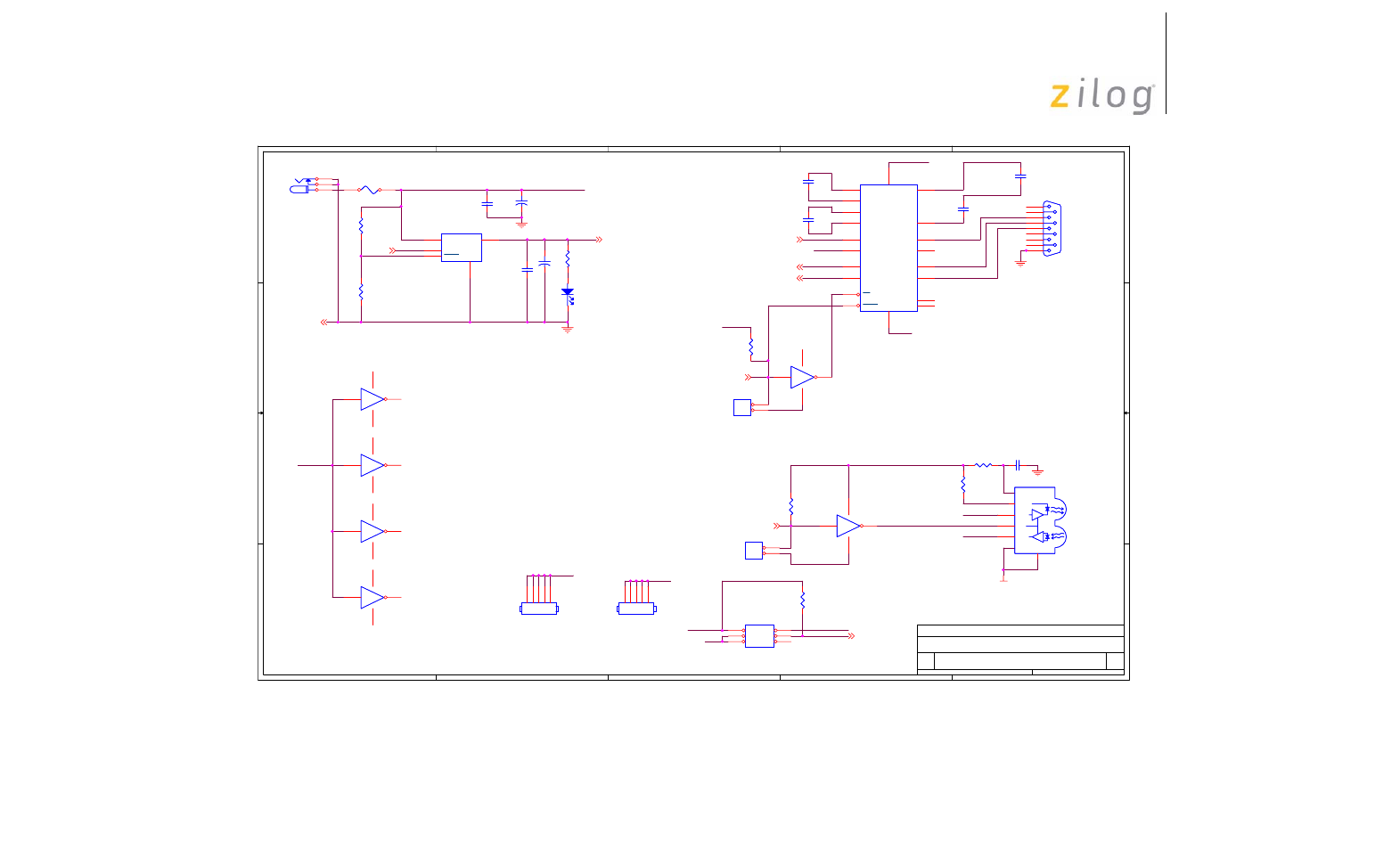
Figure 4. Schematic, Z8 Encore! XP F042A Series MCU Development Board, Page 2 of 2
5
5
4
4
3
3
2
2
1
1
D
D
C
C
B
B
A
A
TXD0
GND
CTS0
RXD0
VCC_33V
DBG
PA4_RXD0
PA5_TXD0
IRDA_SD
GND
PA3_CTS0
VCC_33V
GND
VCC_33V
PA5_TXD0
VCC_33V
PA4_RXD0
GND
VCC_33V
GND
-Z_RST
GND
GND
5V
VCC_33V
VCC
GND
-Z_RST
PA3_CTS0
DBG
-DIS_IRDA
-DIS_232
PA5_TXD0
PA4_RXD0
VCC_33V
GND
SENSE
Title
Size
Document Number
Rev
Date:
Sheet
of
96C0941-001
D
XP 4K MDS Processor Module. Schematic.
B
3
3
Wednesday, March 12, 2008
Title
Size
Document Number
Rev
Date:
Sheet
of
96C0941-001
D
XP 4K MDS Processor Module. Schematic.
B
3
3
Wednesday, March 12, 2008
Title
Size
Document Number
Rev
Date:
Sheet
of
96C0941-001
D
XP 4K MDS Processor Module. Schematic.
B
3
3
Wednesday, March 12, 2008
CONSOLE
GND
USER
DBG
INTERFACE
DIS RS232
DIS IRDA
3.3 OK
C2
0.1uF
C2
0.1uF
R3
68
R3
68
C4
0.1uF
C4
0.1uF
U3E
74LVC04/SO
U3E
74LVC04/SO
11
10
14
7
U3A
74LVC04/SO
U3A
74LVC04/SO
1
2
14
7
U7
LT1129-3.3/DD
U7
LT1129-3.3/DD
OUT
1
SENSE
2
GND
3
SHDN
4
VIN
5
C6
0.1uF
C6
0.1uF
JP3
JP3
1
2
U3D
74LVC04/SO
U3D
74LVC04/SO
9
8
14
7
P2
Header 3x2
P2
Header 3x2
1
2
3
4
5
6
R2
10K
R2
10K
U3B
74LVC04/SO
U3B
74LVC04/SO
3
4
14
7
R23
10K
R23
10K
U3F
74LVC04/SO
U3F
74LVC04/SO
13
12
14
7
C1
0.1uF
C1
0.1uF
JP4
JP4
1
2
C9
330nF
C9
330nF
R1
680
R1
680
F1
RXE050
F1
RXE050
R24
15K
R24
15K
R4
2R7
R4
2R7
C5
0.1uF
C5
0.1uF
J1
PWR JACK
J1
PWR JACK
2
3
1
U4
ZHX1810
U4
ZHX1810
TXD
2
SD
4
RXD
3
LEDA
1
VCC
5
GND
6
T
0
+
C7
100/10
+
C7
100/10
C8
0.1uF
C8
0.1uF
R5
10K
R5
10K
+
C3
100/10
+
C3
100/10
U3C
74LVC04/SO
U3C
74LVC04/SO
5
6
14
7
P1
DB9 Female
P1
DB9 Female
5
9
4
8
3
7
2
6
1
U1
MAX3222
U1
MAX3222
EN
1
C1+
2
C1-
4
C2+
5
C2-
6
T1IN
13
T2IN
12
R1OUT
15
R2OUT
10
V+
3
V-
7
T1OUT
17
T2OUT
8
R1IN
16
R2IN
9
SHDN
20
VCC
19
GND
18
NC
11
NC
14
TP1
TP1
1
2
3
4
5
R6
10K
R6
10K
D1
LED
D1
LED
2
1
TP2
TP2
1
2
3
4
5