Development kit block diagram, Zneo – Zilog Z16F2810 User Manual
Page 8

ZNEO
®
Z16F Series Development Kit
User Manual
UM020205-0908
ZNEO Z16F Series Development Board
4
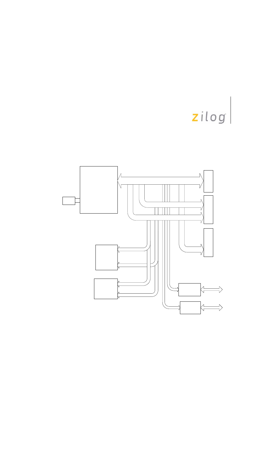
Development Kit Block Diagram
displays the block diagram of ZNEO Z16F Series development
kit.
Figure 2. ZNEO Z16F Series Development Kit Block Diagram
Z8F1285
(128KB FLASH,
4KB SRAM,
12 channel ADC,
3 channel PWM)
FLASH
(1 M x 16, CS0)
SRAM
(256 K x 16, CS1)
IrDA
Ex
te
rn
a
l
GPIO
Bu
s
(J
P
2
)
Ex
te
rn
al
Per
iphera
l
Bu
s
(J
P
1
)
20 MHz
XTAL
RS-232
Externa
l
A
D
C
conne
ct
o
r
(J
P
3)
External Interface Address and Control bus
JP4
ZNEO
®
MCU
External Interface Data bus
GPIO
