Figure 2 figure 3 figure 4, Figure 5 figure 6 – Elenco Deluxe Digital / Analog Trainer with Tools User Manual
Page 7
-6-
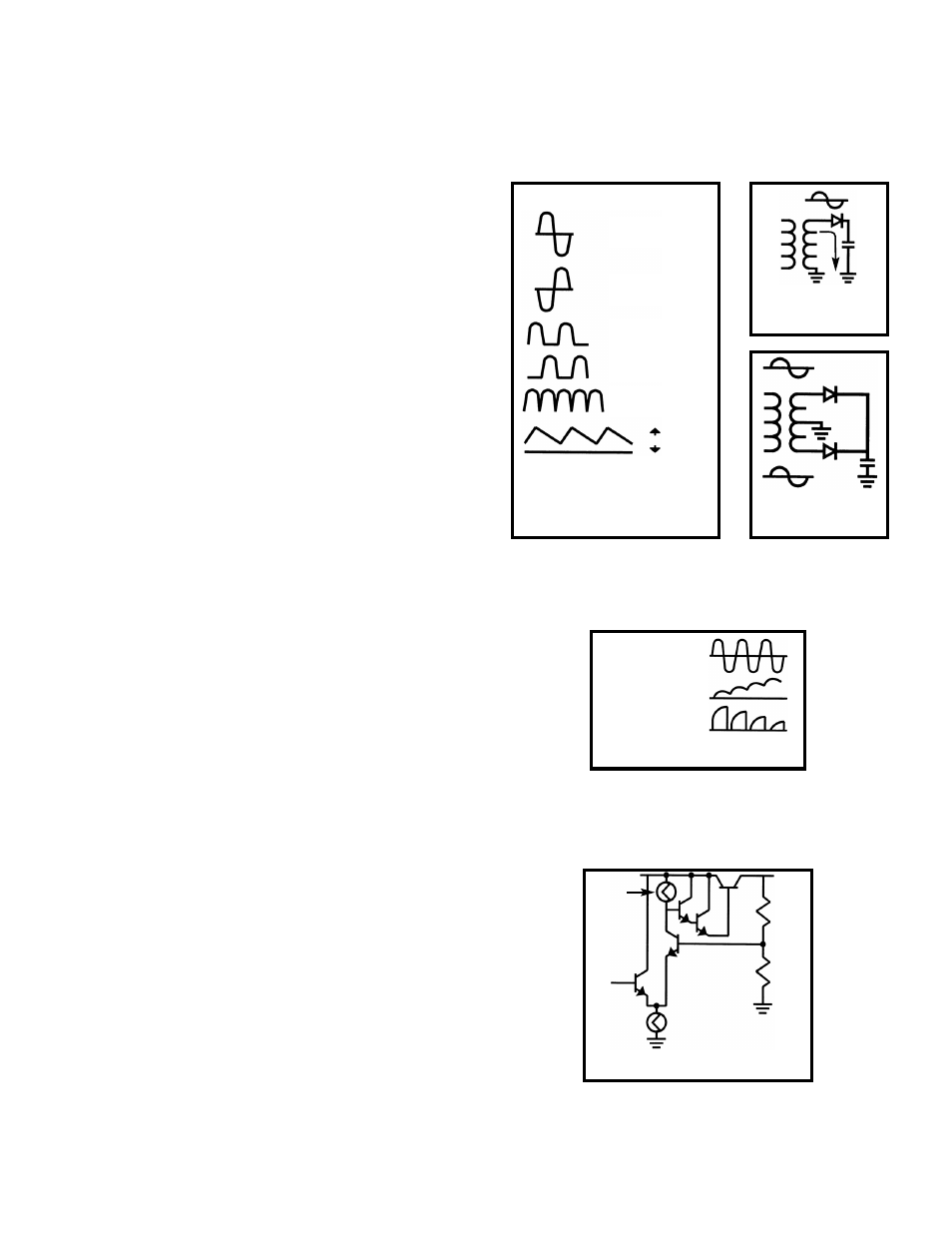
By the addition of a second diode and transformer
winding we can fill in the gap between cycles as
shown in Figure 4. This circuit is called full-wave
rectification. Each diode conducts when the voltage
is positive. By adding the two outputs, the voltage
presented to capacitor C1 is more complete, thus
easier to filter, as shown in Figure 2E. When used
in 60 cycles AC input power, the output of a full
wave rectifier will be 120 cycles.
Capacitor C1 is used to store the current charges,
thus smoothing the DC voltage. The larger the
capacitor, the more current is stored. In this design
1000
μF capacitors are used, which allows about 5
volts AC ripple when one amp is drawn.
In practice, the current through the diodes is not as
shown in Figure 2C. Because capacitor C1 has a
charge after the first cycle, the diode will not
conduct until the positive AC voltage exceeds the
positive charge in the capacitor. Figure 5 shows a
better picture of what the current flow looks like
assuming no loss in the diode.
It takes a few cycles for the voltage to build up on
the capacitor. This depends on the resistance of the
winding and diode. After the initial start-up, there
will be a charge and discharge on the capacitor
depending on the current drawn by the output load.
Remember, current only flows through the diodes
when the anode is more positive than the cathode.
Thus, current will flow in short bursts as shown in
Figure 5.
The DC load current may be one ampere but the
peak diode current may be three times that.
Therefore, the diode rating must be sufficient to
handle the peak current. The 1N4001 has peak
current rating of 10 amps.
REGULATOR CIRCUIT
The regulator circuit in the Model XK-700 power
supply consists of a LM-317 integrated circuit. This
IC is specially designed to perform the regulation
function. Figure 6 shows a simplified circuit of how
the LM-317 IC works.
Transistors Q1 and Q2 form a circuit known as a
differential amplifier. Transistor Q1 base is
connected to a stable 1.5V reference voltage. The
base of Q2 is connected to the regulator output
circuit through a voltage divider network. The
collector of transistor Q2 is connected to a current
source. This basically is a PNP transistor biased to
draw about 1mA current. Transistor Q2 sees the
current source as a very high resistor of about 1
meg ohms. Thus, the gain of transistor Q2 is
extremely high.
A) Transformer
Winding
B) Voltage C1
C) Current
through diodes
20V
Peak
20V
Figure 2
Figure 3
Figure 4
Voltage Waveform for Supply
A) Transformer
Winding AB
B) Transformer
Winding BC
C) Output of
diode D1.
D) Output of
diode D2.
E) Total of diodes
D1 & D2.
20V
F) Output of capacitor C1
Ripple depends on load
current (expanded).
Half Wave Rectifier
Full Wave Rectifier
2V
Output
R1
R2
Divider
Q1
Q2
1.5V
Q3
Q4
Q5
Current
Source
Equalized
to 1 Meg.
Figure 5
Figure 6
D1
D2
C1
C1
D1