Signal descriptions (cont’d) – ADLINK ETX-CV User Manual
Page 28
ETX-CV User’s Manual
Page 28
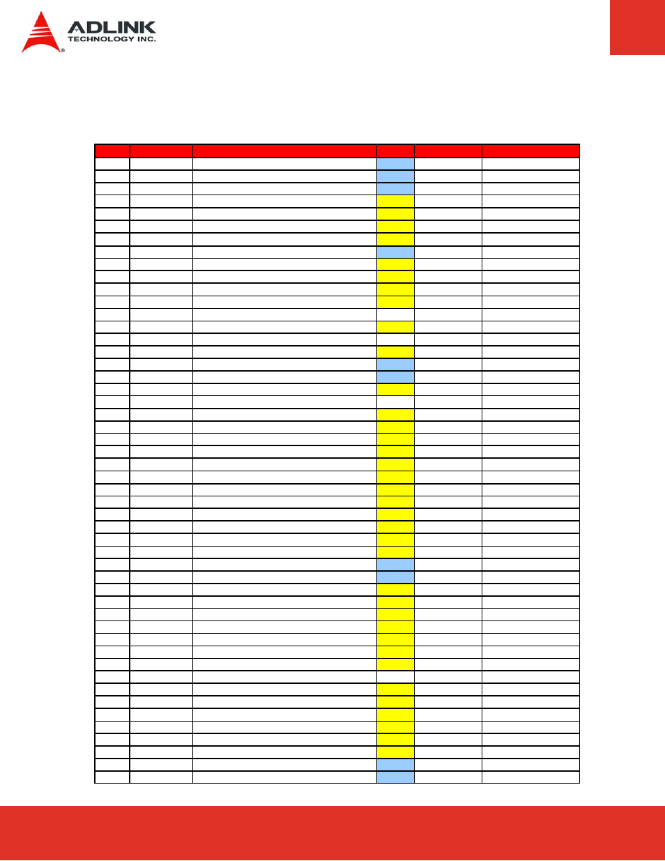
Signal Descriptions (cont’d)
X4
Pin
Signal
Description
Type
PU/PD
Comment
1
GND
Ground
PWR
-
-
2
GND
Ground
PWR
-
-
3
5V_SB
Supply of internal suspend Circuit
PWR
-
-
4
PWGIN
Power Good / Reset Input
I-3,3
-
-
5
PS_ON
Power Supply On
O-5
PU 4k7 3,3VSB
-
6
SPEAKER
Speaker Output
O-5
PU 1k 5V
-
7
PWRBTN#
Power Button
I-5
PU 10k 3,3VSB
-
8
BATT
Battery Supply
PWR
-
-
9
KBINH
Keyboard Inhibit Control Input
I-5
PU 8k2 5V
-
10
LILED
Ethernet Link LED
O-3,3
-
-
11
RSMRST#
Resume Reset input
I-3,3
PU 20k 3,3VSB
-
12
ACTLED
Ethernet Activity LED
O-3,3
-
-
13
ROMKBCS#
-
NC
-
-
14
SPDLED
Ethernet Speed LED
O-3,3
-
-
15
EXT_PRG
-
NC
-
-
16
I2CLK
I2C Bus Clock
O-5
PU 10k 3,3V
17
5VCC
Power +5V
PWR
-
-
18
5VCC
Power +5V
PWR
-
-
19
OVCR#
Over Current Detect for USB
I-3,3
PU 4k7 3,3VSB
-
20
GPCS#
-
NC
-
-
21
EXTSMI#
System Management Interrupt Input
I-3,3
PU 8k2 3,3V
-
22
I2DAT
I2C Bus Data
IO-5
PU 10k 3,3V
-
23
SMBCLK
SM Bus Clock
O-3,3
PU 2k2 3,3V
-
24
SMBDATA
SM Bus Data
IO-3,3
PU 2k2 3,3V
-
25
S_CS3#
Secondary IDE Chip Select Channel 1
O-3,3
-
-
26
SMBALERT
SM Bus Alert
I-3,3
PU 10k 3,3VSB
-
27
S_CS1#
Secondary IDE Chip Select Channel 0
O-3,3
-
-
28
DASP_S
-
I-3,3
PD 10k
-
29
S_A2
Secondary IDE Adress Bus
O-3,3
-
-
30
P_CS3#
Primary IDE Chip Select Channel 1
O-3,3
-
-
31
S_A0
Secondary IDE Adress Bus
O-3,3
-
-
32
P_CS1#
Primary IDE Chip Select Channel 0
O-3,3
-
-
33
GND
Ground
PWR
-
-
34
GND
Ground
PWR
-
-
35
PDIAG_S
80-conductor IDE cable Channel 1
I-3,3
-
-
36
P_A2
Primary IDE Adress Bus
O-3,3
-
-
37
S_A1
Secondary IDE Adress Bus
O-3,3
-
-
38
P_A0
Primary IDE Adress Bus
O-3,3
-
-
39
S_INTRQ
Secondary IDE Interrupt Request
I-3,3
PD 10k
-
40
P_A1
Primary IDE Adress Bus
O-3,3
-
-
41
BATLOW#
Battery Low
I-3,3
-
42
GPE1#
-
NC
-
-
43
S_AK#
Secondary IDE DMA Acknowledge
O-3,3
-
-
44
P_INTRQ
Primary IDE Interrupt Reqeuest
I-3,3
PU 8k2 3,3V
-
45
S_RDY
Secondary IDE Ready
I-3,3
PU 4k7 3,3V
-
46
P_AK#
Primary IDE DMA Acknowledge
O-3,3
-
-
47
S_IOR#
Secondary IDE IO Read
O-3,3
-
-
48
P_RDY
Primary IDE Ready
I-3,3
PU 4k7 3,3V
-
49
5VCC
Power +5V
PWR
-
-
50
5VCC
Power +5V
PWR
-
-