4 board interfaces, 1 cpci-6530v board layout, Chapter 4, board interfaces – ADLINK CT-6530 User Manual
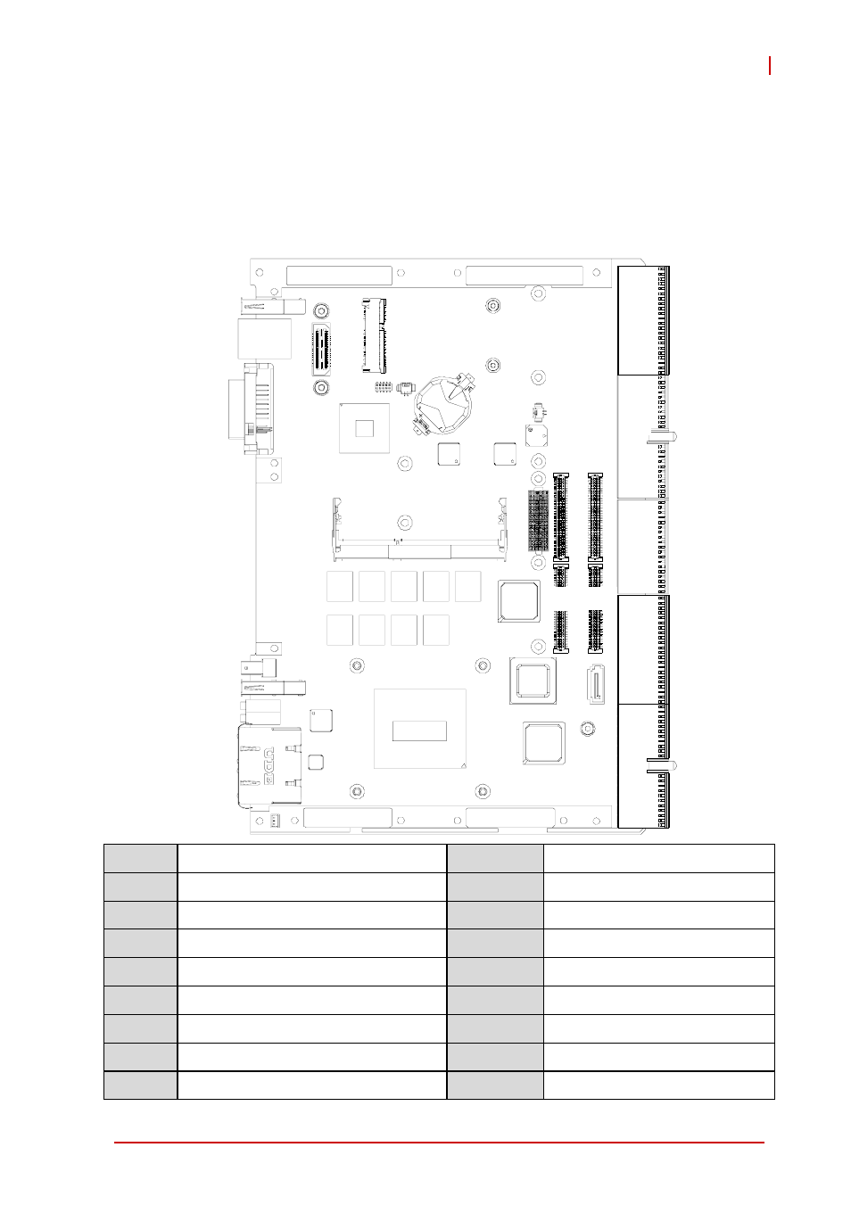
Page 31: Cpci-6530v board layout, Figure 4-1: cpci-6530v series board layout, 4board interfaces

Board Interfaces
19
cPCI-6530
4
Board Interfaces
This chapter illustrates the board layout, connector pin assignments,
and jumper settings to familiarize users with the cPCI-6530 Series.
4.1
cPCI-6530V Board Layout
Figure 4-1: cPCI-6530V Series Board Layout
CPU
Intel® Core
™
Processor
J1~2
CompactPCIconnectors
PCH1
Intel® QM87 PCH
LAN1
Dual Ethernet connectors
CN1
Memory socket
CN9
mSATA connector
CN2
XMC connector
CN10
SATA 7-pin connector
CN4
DVI-I connector
CN11
SATA board-to-board conn.
CN7
COM port in RJ-45 conn.
CN12/13
USB 3.0 connector
BT1
Battery socket
CN14
USB 2.0 connector
U34
PCe Switch PEX8624-BB50BI
JN1/2/3/4
PMC connectors
U23/27 Pericom PI7C9X130
U23/27
Pericom PI7C9X130
J1
CPU1
U27
J2
CN14
CN13
CN11
U34
LAN1
CN4
CN9
BT1
PCH1
CN1
CN2
JN1 JN2
JN3 JN4
U23
CN12
CN7
J3
J4
J5
CN10
