5 software architecture description, 1 functional block diagram, Software architecture description – ADLINK HSL-DI32-M-N/HSL-DI32-M-P User Manual
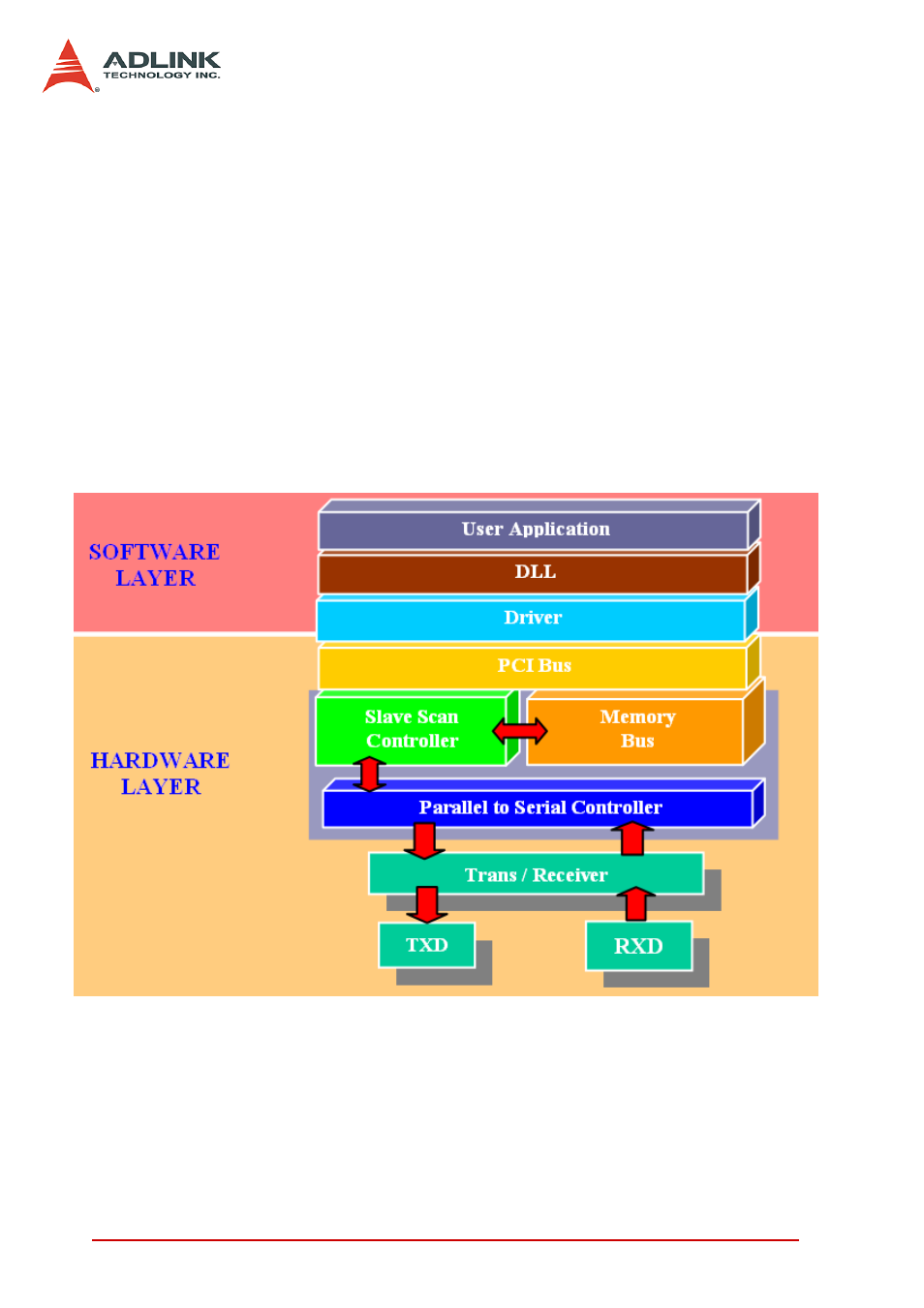
Page 49: Functional block diagram, Figure 2-6: functional block diagram of hsl master

36
HSL Master Controller
2.5 Software Architecture Description
The PCI-7853/PCI-7854/PMC-7852/G comes with one or two HSL
master ASICs that control the HSL communication. The purpose
of communicating with HSL I/O modules is to gather input data
from or set output value to them. To achieve this purpose, each
HSL master controller manages a 2Kbyte SRAM on PCI-7853/
PCI-7854 boards for data storage.
For every polling cycle, the master refreshes all input data from
the I/O modules and sets the latest output data to the I/O modules.
The SRAM keeps these data for the software drivers to read/write
I/O information.
2.5.1 Functional Block Diagram
Figure 2-6: Functional Block diagram of HSL master
The diagram above shows how the HSL communicates with the
user’s AP. The SRAM acts with a buffer-like characteristic.
- USB-1901 (84 pages)
- USB-1210 (54 pages)
- USB-2401 (60 pages)
- USB-7230 (50 pages)
- USB-2405 (56 pages)
- DAQe-2010 (92 pages)
- DAQe-2204 (100 pages)
- DAQe-2213 (94 pages)
- DAQe-2501 (74 pages)
- PXI-2010 (84 pages)
- PXI-2020 (60 pages)
- PXI-2501 (62 pages)
- cPCI-9116 (98 pages)
- ACL-8112 Series (94 pages)
- ACL-8112 Series (92 pages)
- ACL-8112 Series (93 pages)
- ACL-8216 (75 pages)
- ACL-8111 (61 pages)
- PCM-9112+ (10 pages)
- PCM-9112+ (94 pages)
- cPCI-6216V (47 pages)
- ACL-6126 (28 pages)
- ACL-6128A (40 pages)
- PCM-6308V+ (52 pages)
- PCM-6308V+ (4 pages)
- PCI-7444 (82 pages)
- PCI-7434 (48 pages)
- PCI-7234 (56 pages)
- PCI-7260 (66 pages)
- PCI-7258 (38 pages)
- PCI-7256 (48 pages)
- PCI-7250 (48 pages)
- LPCI-7250 (48 pages)
- PCI-7396 (65 pages)
- PCI-7296 (59 pages)
- PCI-8554 (67 pages)
- PCIe-7360 (94 pages)
- PCIe-7350 (86 pages)
- PCIe-7300A (114 pages)
- PCIe-7200 (51 pages)
- PCI-7300A (112 pages)
- PCI-7300A (83 pages)
- PCI-7200 (96 pages)
- cPCI-7300 (82 pages)
- cPCI-7300 (83 pages)
