System reference clock – ADLINK PXIS-2690P User Manual
Page 18

10
Chassis Overview
System Reference Clock
The PXIS-2690P supplies a 10 MHz system reference clock signal
(PXI_CLK10) to every peripheral slot independently. An indepen-
dent buffer (having a source impedance matched to the backplane
and a skew of less than 1 ns between slots) drives the clock signal
to each peripheral slot. You can use this common reference clock
signal to synchronize multiple modules in a measurement or con-
trol system, or drive PXI_CLK10 from an external source through
the PXI_CLK10_IN pin on the P2 connector of the star trigger slot.
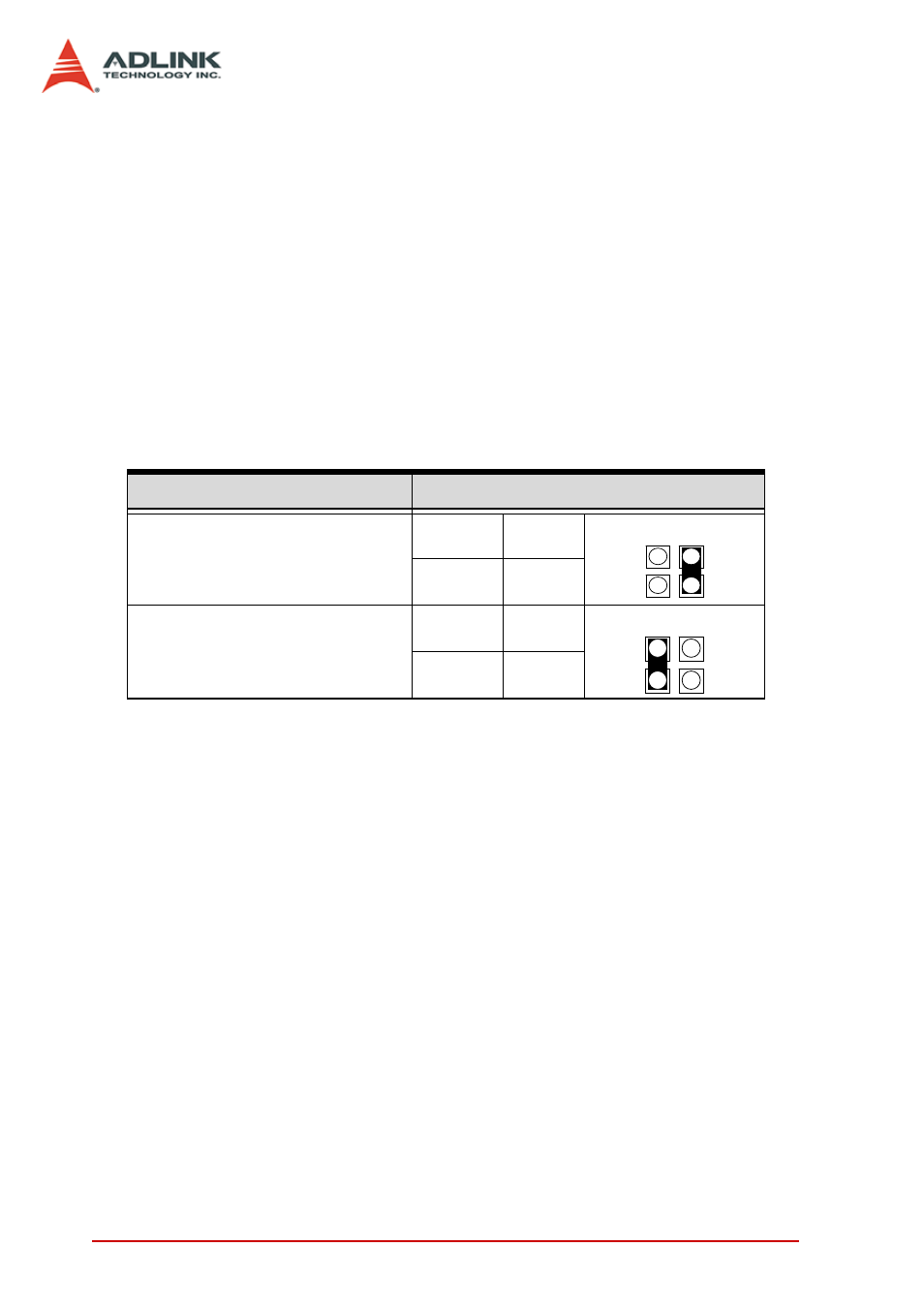
You can select the internal or external clock by setting jumpers
JP2 and JP3 in the backplane rear. Refer to the jumper settings
below.
Description
Jumper Settings
External clock (PXI_CLK10_IN
on star trigger slot)
JP2
Open
JP3
Short
Internal clock (10 MHz system
clock PXI_CLK10)
JP2
Short
JP3
Open
Table 2-1: Reference Clock Jumper Setting
- USB-1901 (84 pages)
- USB-1210 (54 pages)
- USB-2401 (60 pages)
- USB-7230 (50 pages)
- USB-2405 (56 pages)
- DAQe-2010 (92 pages)
- DAQe-2204 (100 pages)
- DAQe-2213 (94 pages)
- DAQe-2501 (74 pages)
- PXI-2010 (84 pages)
- PXI-2020 (60 pages)
- PXI-2501 (62 pages)
- cPCI-9116 (98 pages)
- ACL-8112 Series (93 pages)
- ACL-8112 Series (94 pages)
- ACL-8112 Series (92 pages)
- ACL-8216 (75 pages)
- ACL-8111 (61 pages)
- PCM-9112+ (10 pages)
- PCM-9112+ (94 pages)
- cPCI-6216V (47 pages)
- ACL-6126 (28 pages)
- ACL-6128A (40 pages)
- PCM-6308V+ (52 pages)
- PCM-6308V+ (4 pages)
- PCI-7444 (82 pages)
- PCI-7434 (48 pages)
- PCI-7234 (56 pages)
- PCI-7260 (66 pages)
- PCI-7258 (38 pages)
- PCI-7256 (48 pages)
- PCI-7250 (48 pages)
- LPCI-7250 (48 pages)
- PCI-7396 (65 pages)
- PCI-7296 (59 pages)
- PCI-8554 (67 pages)
- PCIe-7360 (94 pages)
- PCIe-7350 (86 pages)
- PCIe-7300A (114 pages)
- PCIe-7200 (51 pages)
- PCI-7300A (112 pages)
- PCI-7300A (83 pages)
- PCI-7200 (96 pages)
- cPCI-7300 (82 pages)
- cPCI-7300 (83 pages)
