5 setting linear address (j1 & j2), 6 setting clock source (j3), 7 de/e signal from m or lp (j4) – Acrosser AR-B1042 User Manual
Page 16

AR-B1042 User
s Guide
2-6
Name Description
-MASTER [Input]
The MASTER is the signal from the I/O processor which
gains control as the master and should be held low for a
maximum of 15 microseconds or system memory may be
lost due to the lack of refresh
-MEMCS16
[Input, Open collector]
The Memory Chip Select 16 indicates that the present
data transfer is a 1-wait state, 16-bit data memory
operation
-IOCS16
[Input, Open collector]
The I/O Chip Select 16 indicates that the present data
transfer is a 1-wait state, 16-bit data I/O operation
OSC [Output]
The Oscillator is a 14.31818 MHz signal
-ZWS
[Input, Open collector]
The Zero Wait State indicates to the microprocessor that
the present bus cycle can be completed without inserting
additional wait cycle
Table 2-1 I/O Channel Pin Assignment
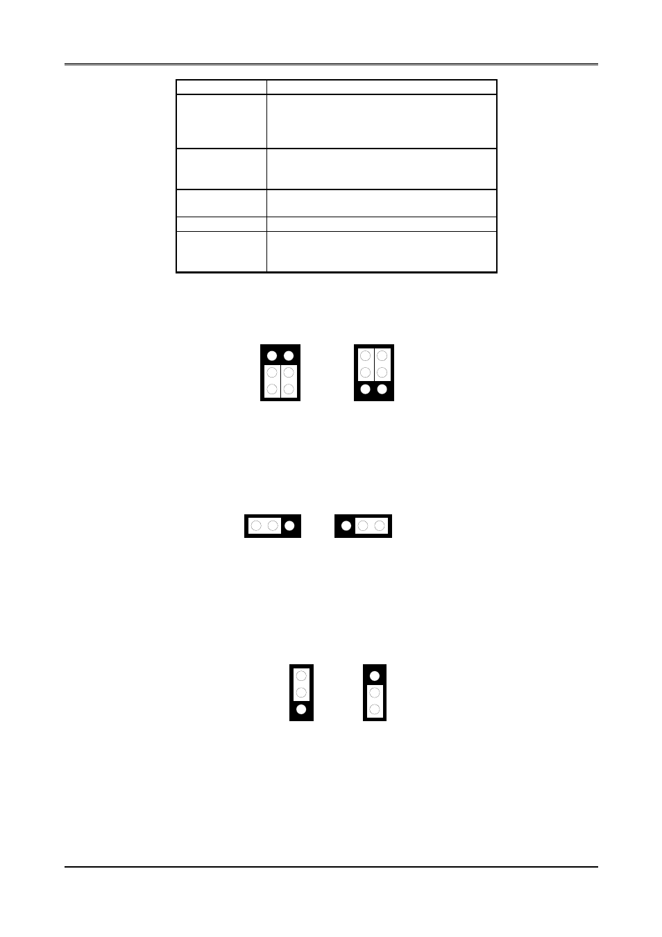
2.2.5 Setting Linear Address (J1 & J2)
3
2
J1
1
J2
3
1
2
Linear Address
Factory Preset
3
2
J1
1
J2
3
1
2
Non-Linear Address
Figure 2-7 J1 & J2: Setting Linear Address
2.2.6 Setting Clock Source (J3)
1 2
On-Board
Factory Preset
J3
1
2
PC/104 Bus (System)
3
3
Figure 2-8 J3: Setting Clock Source
2.2.7 DE/E Signal from M or LP (J4)
1
2
DE/M
Factory Preset
J4
1
2
E/LP
3
3
Figure 2-9 J4: DE/E Signal from M or LP Select
