Figure 5, Psoc device internals – Cypress CY8C29x66 User Manual
Page 8

AN2309
November 25, 2007
Document No. 001-17394 Rev. *B
- 8 -
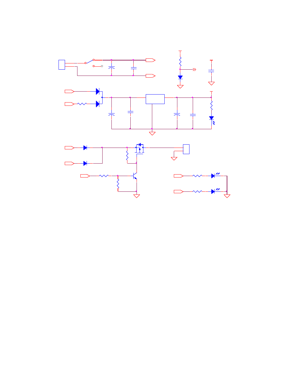
Figure 5. Two-Cell Battery Charger Schematic
– Power Supply and User Interface
R30
33
1
2
J4
POWER 12V DC
PSoC
C12
0.33u 16V
IN
1
OUT
3
U2 L78L05/TO
D6
BAT54C
Close to PSoC
C15
0.1u
D8
BAS16
VCC
R29
1K
VCC
Vbias
POWER-
+
C9
100u 16V
C10
0.1u 16V
+
POWER+
SW1
POWER+
C14
0.1u
+
C13
22u
VCC
+
C11
100u 16V
D7
POWER
R28
470
BAT+
Q6
IRLML6402
LOAD_EN
R25
1M
R26
330R
Q7
BC817
R27
10K
1
2
J3
LOAD
BAT+
POWER+
D4
MBR360
D5
MBR360
D2
LED
R2
470
LED_Y ELLOW
D3
LED
R3
470
LED_GREEN
PSoC Device Internals
The internal structure of the PSoC device is shown in
on page 9. The PWM is placed on DBB01 and DCB02.
The module is configured in the software as an 11-bit PWM,
which provides for a sufficient number of regulation steps.
The TIMER User Module is based on the internal sleep
timer and configured to generate interrupts every one
second. This real clock is used to calculate other time
intervals. The serial transmitter is placed into DCB03. The
default exchange speed is set to 115200 baud.
The cell-balancing MOSFETS Q4, Q5 are controlled directly
from the CPU (high level - close, low level - open).
The three-opamp topology of the instrumental amplifier
(INA) is used in this implementation. The INA is placed in
ACB00, ACB01, and ASD11. The incremental ADC is
placed in the ASC10 and DBB00 blocks.
The ADC resolution is set to 12 bits, and the integration time
is adjusted to be precisely equal to the integer number of the
PWM signal. All of the switched capacitor user modules use
the same column frequency to eliminate aliasing problems.
In this project, the analog ground bias was set to bandgap or
1.3V (RefMux is BandGap ± BandGap).
Note that if you require more program memory and analog
pins, or require USB support, in your user-defined projects,
you can import this charger to the CY8C24794 or the
CY8C27x43 PSoC device family. The CY8C24794 device
includes a full-featured, full-speed (12 Mbps) USB port and
can have up to seven IO ports that connect to the global
digital and analog interconnects, providing access to four
digital blocks and six analog blocks. For additional
information, see “Products: PSoC Mixed-Signal Controllers:
PSoC
Mixed-
Signal
Array:
CY8C24794”
on
