Block diagram, I/o connections – AJA R10CE User Manual
Page 4
4
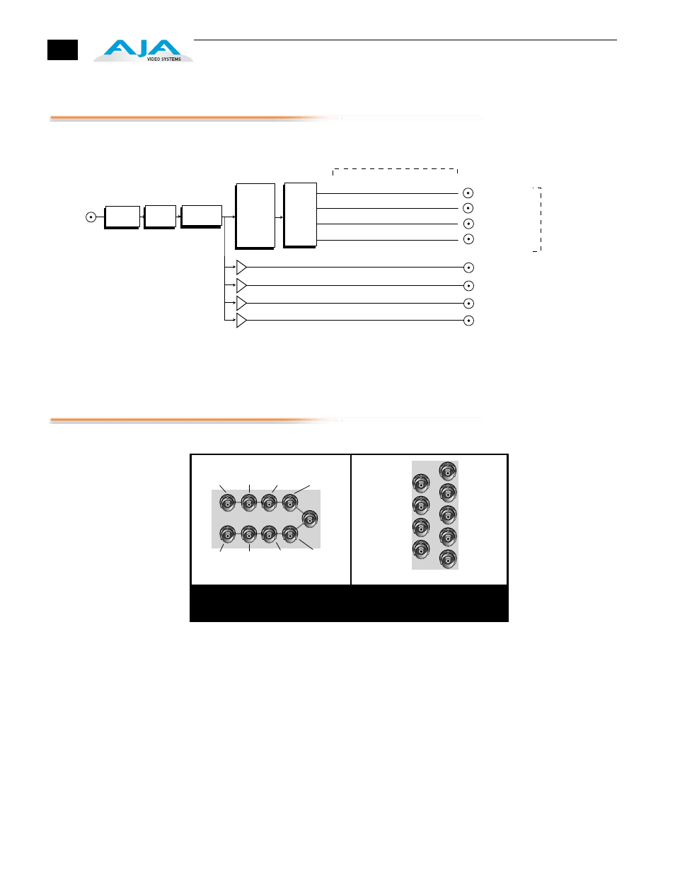
Block Diagram
R10CE Monitoring Digital DA, Simplified Block Diagram
I/O Connections
FR1 and FR2 BNC Connector Assignments, R10CE Card Module
When the R10CE module is installed in an AJA FR1 or FR2 frame, a corresponding
group of 9 BNCs on the rear panel then provide I/O for the module. The
illustration above shows the connector assignments for both the FR1 and FR2
when used with the R10CE.
SD Input
Analog
(Component or
Composite)
ReClock
Cable EQ
Comp/-/G/Y Out
Comp Out
Comp/Y/B/B-Y Out
Comp/C/R/R-Y Out
Set by
Switches
Y G - Composite
Composite
Pb B Y Composite
Pr R C Composite
Cable
Drivers
D/A
Conversion
Deserializer
Serial Out 1
Serial Out 2
Serial Out 3
Serial Out 4
PLL
Jitter
Filter
J1
J3
J5
J7
J9
J2
J4
J6
J8
J1
J2
J3
J4
J5
J6
J7
J8
J9
FR1 Frame Layout
R5CE Rear Panel
FR2 Frame Layout
R5CE Rear Panel
SDI In
SDI Out 2
SDI Out 4
Comp
Out
Comp/Y/B/
Pb Out
SDI Out 1
SDI Out 3
Comp/
-/G/Y Out
Comp/
C/R/Pr
Out
SDI In
SDI
Out 2
SDI
Out 1
SDI
Out 4
SDI Out 3
Comp
Out
Comp/Y/B/
Pb Out
Comp/
C/R/Pr
Out
Comp/
-/G/Y
Out