Block diagram, I/o connections, Rh10md, block diagram – AJA RH10MD User Manual
Page 4
4
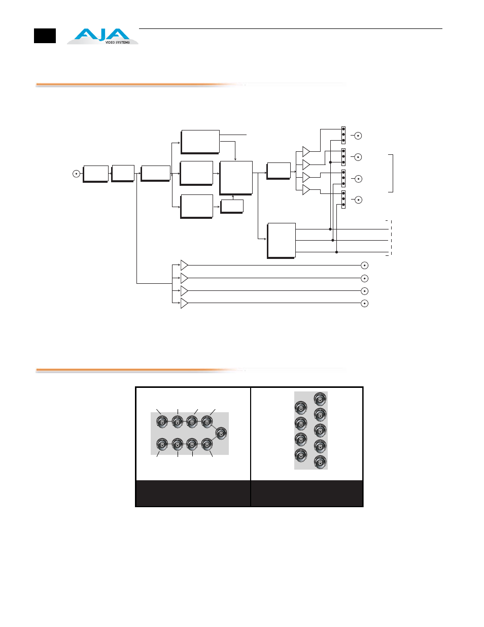
Block Diagram
RH10MD, Block Diagram
I/O Connections
FR1 and FR2 BNC Connector Assignments, RH10MD Card Module
When the RH10MD module is installed in an AJA FR1 or FR2 frame, a
corresponding group of 9 BNCs on the rear panel then provide I/O for the
module. The illustration above shows the connector assignments for both the
FR1 and FR2 when used with the RH10MD.
Output configuration is discussed next in
User Controls
.
HD or
SD Input
Any Output
can be
configured as
SD or Analog
(Component or
Composite)
ReClock
Cable EQ
SD Out 2
SD Out 1
SD Out 3
SD Out 4
Set by
Switches
Y G Composite Composite
Pb B Y Composite
Pr R C Composite
Cable
Drivers
D/A
Conversion
H & V
Filtering and
Decimation
Embedded
Audio
Extraction
Deserializer
Delay
Serializer
3
2
1
DA 1
DA 2
DA 3
DA 4
4
5
6
3
2
1
4
5
6
3:2 Pulldown
Synchronization
RP188/RP215
Timecode
Extraction
Audio
Embedding &
RP188
Timecode
Embedding
J1
J3
J5
J7
J9
J2
J4
J6
J8
J1
J2
J3
J4
J5
J6
J7
J8
J9
FR1 Frame Layout
RH10MD Rear Panel
FR2 Frame Layout
RH10MD Rear Panel
Input
DA Out 2
DA Out 4
SD Out 1
SD Out 3
DA Out 1
DA Out 3
SD Out 2
SD Out 4
Input
DA Out
2
DA Out
1
DA Out
4
DA Out
3
SD
Out 1
SD
Out 3
SD
Out 2
SD
Out 4