Analog Devices MicroConverter ADuC824 User Manual
Page 2
(not used)
(not used)
(not used)
(not used)
(not used)
(not used)
(not used)
(not used)
(not used)
(not used)
(not used)
(not used)
(not used)
(not used)
(not used)
(not used)
(not used)
(not used)
(reserved)
(reserved)
(reserved)
(reserved)
(reserved)
(reserved)
(reserved)
(reserved)
(reserved)
(reserved)
(reserved)
(reserved)
(reserved)
(reserved)
(reserved)
(reserved)
(reserved)
(reserved)
(reserved)
(reserved)
(reserved)
(reserved)
(reserved)
(reserved)
(reserved)
(reserved)
(reserved)
(reserved)
(reserved)
(reserved)
(reserved)
(reserved)
(reserved)
(reserved)
(reserved)
(reserved)
(reserved)
(reserved)
(reserved)
(reserved)
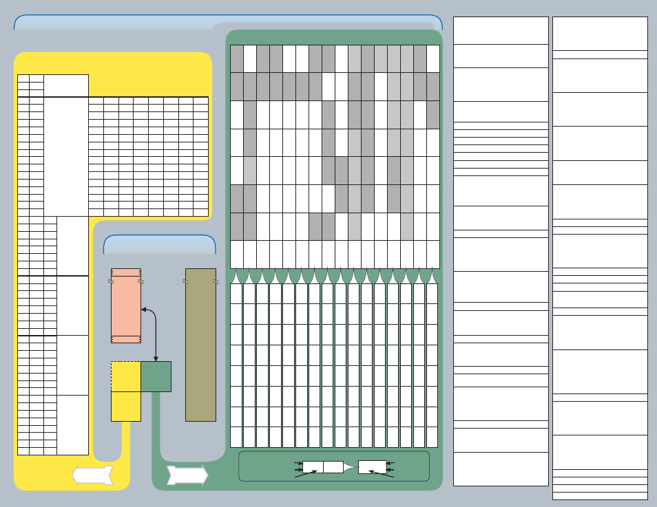
7Fh
...
30h
2Fh
2Eh
2Dh
2Ch
2Bh
2Ah
29h
28h
27h
26h
25h
24h
23h
22h
21h
20h
1Fh
R7
1Eh
R6
1Dh
R5
1Ch
R4
1Bh
R3
1Ah
R2
19h
R1
18h
R0
17h
R7
16h
R6
15h
R5
14h
R4
13h
R3
12h
R2
11h
R1
10h
R0
0Fh
R7
0Eh
R6
0Dh
R5
0Ch
R4
0Bh
R3
0Ah
R2
09h
R1
08h
R0
07h
R7
06h
R6
05h
R5
04h
R4
03h
R3
02h
R2
01h
R1
00h
R0
General Purpose
Area
Bit Addressable
Area
Register
Bank 3
Register
Bank 2
Register
Bank 1
Register
Bank 0
7Fh
7Eh
7Dh
7Ch
7Bh
7Ah
79h
78h
77h
76h
75h
74h
73h
72h
71h
70h
6Fh
6Eh
6Dh
6Ch
6Bh
6Ah
69h
68h
67h
66h
65h
64h
63h
62h
61h
60h
5Fh
5Eh
5Dh
5Ch
5Bh
5Ah
59h
58h
57h
56h
55h
54h
53h
52h
51h
50h
4Fh
4Eh
4Dh
4Ch
4Bh
4Ah
49h
48h
47h
46h
45h
44h
43h
42h
41h
40h
3Fh
3Eh
3Dh
3Ch
3Bh
3Ah
39h
38h
37h
36h
35h
34h
33h
32h
31h
30h
2Fh
2Eh
2Dh
2Ch
2Bh
2Ah
29h
28h
27h
26h
25h
24h
23h
22g
21h
20h
1Fh
1Eh
1Dh
1Ch
1Bh
1Ah
19h
18h
17h
16h
15h
14h
13h
12h
11g
10h
0Fh
0Eh
0Dh
0Ch
0Bh
0Ah
09h
08h
07h
06h
05h
04h
03h
02h
01h
00h
127
...
48
47
46
45
44
43
42
41
40
39
38
37
36
35
34
33
32
31
30
29
28
27
26
25
24
23
22
21
20
19
18
17
16
15
14
13
12
11
10
9
8
7
6
5
4
3
2
1
0
decimal
address
HEX
address
(bit addresses)
SFRs
(direct
addressing
only)
128 bytes
upper RAM
(indirect
addressing
only)
128 bytes
lower RAM
(direct or
indirect
addressing)
640 bytes
(160 pages)
data
Flash/EE
(accessible
through
SFRs)
external
data
memory
(16MEG
addressable)
SFR details
lower RAM
details
SPICON
F8h
04h
B
F0h
00h
DCON
E8h
00h
ACC
E0h
00h
ADCST
A
T
D8h
00h
PSW
D0h
00h
T2CON
C8h
00h
WDCON
C0h
10h
IP
B8h
00h
P3
B0h
FFh
IE
A8h
00h
P2
A0h
FFh
SCON
98h
00h
P1
90h
FFh
TCON
88h
00h
P0
80h
FFh
ADC0L
D9h
00h
ECON
B9h
00h
IEIP2
A9h
A0h
SBUF
99h
00h
TMOD
89h
00h
SP
81h
07h
ADC0M
DAh
00h
ADC0CON
D2h
07h
RCAP2L
CAh
00h
TL0
8Ah
00h
DPL
82h
00h
DACL
FBh
00h
ADC1CON
D3h
00h
RCAP2H
CBh
00h
TL1
8Bh
00h
DPH
83h
00h
DACH
FCh
00h
SF
D4h
45h
TL2
CCh
00h
EDA
T
A1
BCh
00h
TH0
8Ch
00h
DPP
84h
00h
DACCON
FDh
00h
TH2
CDh
00h
EDA
T
A2
BDh
00h
TH1
8Dh
00h
EADRL
C6h
00h
EDA
T
A3
BEh
00h
SPIDA
T
F7h
00h
PSMCON
DFh
DEh
EDA
T
A4
BFh
00h
PCON
87h
00h
SPR0
F8h
0
F0h
0
E8h
0
E0h
0
D8h
0
P
D0h
0
CAP2
C8h
0
WDWR
C0h
0
PX0
B8h
0
RXD
B0h
1
EX0
A8h
0
A0h
1
RI
98h
0
T2
90h
1
IT0
88h
0
80h
1
SPR1
F9h
0
F1h
0
E9h
0
E1h
0
D9h
0
F1
D1h
0
CNT2
C9h
0
WDE
C1h
0
PT0
B9h
0
TXD
B1h
1
ET0
A9h
0
A1h
1
TI
99h
0
T2EX
91h
1
IE0
89h
0
81h
1
CPHA
F
Ah
1
F2h
0
EAh
0
E2h
0
ERR1
DAh
0
OV
D2h
0
TR2
CAh
0
WDS
C2h
0
PX1
BAh
0
INT0
B2h
1
EX1
AAh
0
A2h
1
RB8
9Ah
0
92h
1
IT1
8Ah
0
82h
1
CPOL
FBh
0
F3h
0
D0EN
EBh
0
E3h
0
ERR0
DBh
0
RS0
D3h
0
EXEN2
CBh
0
WDIR
C3h
0
PT1
BBh
0
INT1
B3h
1
ET1
ABh
0
A3h
1
TB8
9Bh
0
93h
1
IE1
8Bh
0
83h
1
SPIM
FCh
0
F4h
0
ECh
0
E4h
0
NOXREF
DCh
0
RS1
D4h
0
TCLK
CCh
0
PRE0
C4h
1
PS
BCh
0
T0
B4h
1
ES
ACh
0
A4h
1
REN
9Ch
0
94h
1
TR0
8Ch
0
84h
1
SPE
FDh
0
F5h
0
D0
EDh
0
E5h
0
CAL
DDh
0
F0
D5h
0
RCLK
CDh
0
PRE1
C5h
0
PT2
BDh
0
T1
B5h
1
ET2
ADh
0
A5h
1
SM2
9Dh
0
95h
1
TF0
8Dh
0
85h
1
WCOL
FEh
0
F6h
0
D1EN
EEh
0
E6h
0
RDY1
DEh
0
AC
D6h
0
EXF2
CEh
0
PRE2
C6h
0
P
ADC
BEh
0
WR
B6h
1
EADC
AEh
0
A6h
1
SM1
9Eh
0
96h
1
TR1
8Eh
0
86h
1
ISPI
FFh
0
F7h
0
D1
EFh
0
E7h
0
RDY0
DFh
0
CY
D7h
0
TF2
CFh
0
PRE3
C7h
0
BFh
0
RD
B7h
1
EA
AFh
0
A7h
1
SM0
9Fh
0
97h
1
TF1
8Fh
0
87h
1
MSB
address
LSB
address
00h
000000h
FFFFFFh
FFh
9Fh
00h
( page 0 )
( page 159 )
SPR0
F8h
0
SPICON
F8h
00h
SPR1
F9h
0
mnemonic
reset value
address
mnemonic
address
reset value
these bits
this byte
are contained in
*
calibration coefficients are preconfigured at power-up to factory calibrated values
ADC0H
DBh
00h
ADC1L
DCh
00h
ADC1H
DDh
00h
ICON
D5h
00h
ADCMODE
D1h
00h
GN0L
*
E9h
~55h
GN0M
*
EAh
~55h
OF0M
E2h
00h
OF0H
E3h
80h
OF1L
E4h
00h
GN0H
*
EBh
~53h
GN1L
*
ECh
~9Ah
GN1H
*
EDh
~59h
OF1H
E5h
80h
OF0L
E1h
00h
PLLCON
D7h
03h
CHIPID
C2h
06h
TIMECON
A1h
00h
HTHSEC
A2h
00h
SEC
A3h
00h
MIN
A4h
00h
HOUR
A5h
00h
INTV
AL
A6h
00h
DACCON.4
DAC pin select bit [0=pin3 / 1=pin12]
DACCON.3
ModeSelect (0=12bit, 1=8bit)
DACCON.2
RangeSelect (0=2.5V, 1=AV
DD
)
DACCON.1
Clear DAC (0=0V, 1=normal operation)
DACCON.0
PowerDown DAC (0=off, 1=on)
ISPI
SPI inturrupt (set at end of SPI transfer)
WCOL
write collision error flag
SPE
SPI enable (0=DCON enable, 1=SPI enable)
SPIM
master mode select (0=slave)
CPOL
clock polarity select (0=SCLK idles low)
CPHA
clock phase select (0=leading edge latch)
SPR1
SPI bitrate select bits
SPR0
bitrate = F
CORE
/ [2, 4, 8, 16]
AD0CON.7
(this bit must contain zero)
AD0CON.6
external reference select bit (0=internal ref)
AD0CON.5
channel selection bits:
AD0CON.4
[AIN1-AIN2,AIN3-AIN4,AIN2-AIN2,AIN3-AIN2]
AD0CON.3
unipolar select bit (0=bipolar)
AD0CON.2
range select bits:
AD0CON.1
[±20mV, ±40mV, ±80mV, ±160mV, ±320mV,
AD0CON.0
±640mV, ±1.28V, ±2.56V]
RDY0
primary ADC ready flag
RDY1
auxiliary ADC ready flag
CAL
calibration flag
NOXREF
no external reference flag
ERR0
primary ADC error flag
ERR1
auxiliary ADC error flag
DACCON
DAC Control register
SF
Sync Filter Register: f
ADC
= 4,096Hz ÷ (3·SF)
SPICON
SPI Control register
SPIDAT
SPI Data register
ADC0CON
Primary ADC Control Register
B
auxiliary math register
ADCSTAT
ADC Status Register
ACC
Accumulator
PSMCON
Power Supply Monitor control register
PSMCON.7
DV
DD
compare bit (0=fault)
PSMCON.6
AV
DD
compare bit (0=fault)
PSMCON.5
PSM interrupt bit
PSMCON.4
DV
DD
trip point select bits
PSMCON.3
[4.63V, 3.08V, 2.93V, 2.63V]
PSMCON.2
AV
DD
trip point select bits
PSMCON.1
[4.63V, 3.08V, 2.93V, 2.63V]
PSMCON.0
PSM powerdown control (1=on / 0=off)
ADCMODE
ADC Mode Register
ADMODE.5
primary ADC enable bit
ADMODE.4
auxiliary ADC enable bit
ADMODE.2
mode bits
ADMODE.1
[powerdown, idle, sngl-conv, cont-conv,
ADMODE.0
zero-selfcal, fs-selfcal, zero-syscal, fs-syscal]
ADC1CON
Auxiliary ADC Control Register
CY
carry flag
AC
auxiliary carry flag
F0
general purpose flag 0
RS1
register bank select control bits
RS0
active register bank = [0,1,2,3]
OV
overflow flag
F1
general purpose flag 1
P
parity of ACC
DACH
,
DACL
DAC data registers
PSW
Program Status Word
TH2,TL2
Timer2 register
RCAP2H,RCAP2L
Timer2 Reload/Capture
TF2
overflow flag
EXF2
external flag
RCLK
receive clock enable (0=Timer1 used for RxD clk)
TCLK
transmit clock enable (0=Timer1 used for TxD clk)
EXEN2
external enable (0=ignore T2EX, 1=cap/rld on T2EX)
TR2
run control (0=stop, 1=run)
CNT2
timer/counter select (0=timer, 1=counter)
CAP2
capture/reload select (0=reload, 1=capture)
T2CON
Timer2 Control register
EADRH
,
EADRL
Data Flash/EE address registers
PRE3
watchdog timeout selection bits
PRE2
0000-0111 = timeout=[15.6, 31.2, 62.5, 125, 500
PRE1
1000 = immediate reset
1000, 2000] ms
PRE0
all others codes = reserved
WDIR
watchdog interrupt response enable
WDS
watchdog status flag
WDE
watchdog enable
WDWR
watchdog write enable
WDCON
Watchdog Timer control register
EDATA1
,
EDATA2
,
EDATA3
,
EDATA4
Data Flash/EE data registers
01h READ page
02h PROGRAM page
04h VERIFY page
05h ERASE page
06h ERASE ALL
ECON
Data Flash/EE comand register
IP.7
(not used)
PADC
priority of RDY0/RDY1 (ADC interrupt)
PT2
priority of TF2/EXF2 (Timer2 overflow interrupt)
PS
priority of RI/TI (serial port interrupt)
PT1
priority of TF1 (Timer1 overflow interrupt)
PX1
priority of IE1 (external INT1)
PT0
priority of TF0 (Timer0 overflow interrupt)
PX0
priority of IE0 (external INT0)
IP
Interrupt Priority register
RD
external data memory read strobe
WR
external data memory write strobe
T1
timer/counter 1 external input
T0
timer/counter 0 external input
INT1
external interrupt 1
INT0
external interrupt 0
TxD
serial port transmit data line
RxD
serial port receive data line
P3
Port3 register
IEIP2.7
(not used)
IEIP2.6
pirority of TII interrupt (timer interval)
IEIP2.5
priority of PSMI interrupt (power supply monitor)
IEIP2.4
priority of ISPI interrupt (serial interface)
IEIP2.3
(this bit must contain zero)
IEIP2.2
enable TII interrupt (timer interval)
IEIP2.1
enable PSMI interrupt (power supply monitor)
IEIP2.0
enable ISPI interrupt (serial interface)
IEIP2
Interrupt Enable/Priority register #2
EA
enable inturrupts (0=all inturrupts disabled)
EADC
enable RDY0/RDY1 (ADC interrupt)
ET2
enable TF2/EXF2 (Timer2 overflow interrupt)
ES
enable RI/TI (serial port interrupt)
ET1
enable TF1 (Timer1 overflow interrupt)
EX1
enable IE1 (external interrupt 1)
ET0
enable TF0 (Timer0 overflow interrupt)
EX0
enable IE0 (external interrupt 0)
IE
Interrupt Enable register #1
P2
Port2 register
SBUF
Serial port Buffer register
SM0
UART mode control bits
baud rate:
SM1
00 - 8bit shift register - F
CORE
/12
01 - 8bit UART
- TimerOverflowRate/32(x2)
10 - 9bit UART
- F
CORE
/64(x2)
11 - 9bit UART
- TimerOverflowRate/32(x2)
SM2
in modes 2&3, enables multiprocessor communication
REN
receive enable control bit
TB8
in modes 2&3, 9th bit transmitted
RB8
in modes 2&3, 9th bit received
TI
transmit interrupt flag
RI
receive interrupt flag
SCON
Serial communications Control register
P1.2-1.7 analog/digital pins (1=analog function, 0=digital input)
T2EX
timer/counter 2 capture/reload trigger (or digital I/O)
T2
timer/counter 2 external input (or digital I/O)
P1
Port1 register
TH0,TL0
Timer0 registers
TH1,TL1
Timer1 registers
TMOD.3/.7
gate control bit (0=ignore INTx)
TMOD.2/.6
counter/timer select bit (0=timer)
TMOD.1/.5
timer mode selecton bits
TMOD.0/.4
[13bitT, 16bitT/C, 8bitT/Creload, 2x8bitT]
(upper nibble = Timer1, lower nibble = Timer0)
TMOD
Timer Mode register
TF1
Timer1 overflow flag
TR1
Timer1 run control (0=off, 1=run)
TF0
Timer0 overflow flag
TR0
Timer0 run control (0=off, 1=run)
IE1
external INT1 flag
IT1
IE1 type (0=level trig, 1=edge trig)
IE0
external INT0 flag
IT0
IE0 type (0=level trig, 1=edge trig)
TCON
Timer Control register
PCON.7 double baud rate control
PCON.6 enable serial interrupt (ISI) from power-down mode
PCON.5 enable interrupt 0 (INT0) from power-down mode
PCON.4 ALE disable (0=normal, 1=forces ALE high)
PCON.3 general purpose flag
PCON.2 general purpose flag
PCON.1 power-down control bit (0=normal)
PCON.0 idle-mode control (0=normal)
PCON
Power Control register
DPP
Data Pointer Page
DPH,DPL (DPTR)
Data Pointer
SP
Stack Pointer
P0
Port0 register
81h READ byte
82h PROGRAM byte
0Fh EXIT ULOAD mode
F0h ENTER ULOAD mode
(all others reserved)
AD1CON.6
external reference select bit (0=internal ref)
AD1CON.5
channel selection bits:
AD1CON.4
[AIN3, AIN4, TEMP, AIN5]
AD1CON.3
unipolar select bit (0 = bipolar)
ICON.6
burnout current enable bit
ICON.5
ADC1 current correction bit (0=correction off)
ICON.4
ADC0 current correction bit (0=correction off)
ICON.3
I2 pin select bit [0=pin4 / 1=pin3]
ICON.2
I1 pin select bit [0=pin3 / 1=pin4]
ICON.1
I2 enable bit (0=disable)
ICON.0
I1 enable bit (0=disable)
ICON
Current Source Control Register
PLLCON.7
oscillator powerdown control bit (0=normal)
PLLCON.6
PLL lock indicator flag (0=out of lock)
PLLCON.5
(this bit must contain zero)
PLLCON.4
EA detect status bit (reflects state of EA pin)
PLLCON.3
“fast interrupt” control bit (0=normal)
PLLCON.2
3-bit clock divideer value, “CD” (default=3):
PLLCON.1
PLLCON.0
PLLCON
PLL Control Register
f
CORE
= 12,582,912Hz ÷ 2
CD
CHIPID
Chip ID Register
(0X hex = ADuC824)
TIMECON.6 24hour select bit (0=255hour)
TIMECON.5 interval timebase select bits
TIMECON.4 [128th sec, seconds, minutes, hours]
TIMECON.3 single time interval control bit (0=reload&restart)
TIMECON.2 time interval interrupt bit, “TII”
TIMECON.1 time interval enable bit (0=disable&clear)
TIMECON.0 time clock enable bit (0=disable)
TIMECON
Time Interval Counter Control Register
HTHSEC
TIC Elapsed 128th Second Register
SEC
TIC Elapsed Seconds Register
MIN
TIC Elapsed Minutes Register
HOUR
TIC Elapsed Hours Register
INTVAL
TIC Interval Register
OF0H
,
OF0M
,
OF0L
ADC0 offset coefficient
OF1H
,
OF1L
ADC1 offset coefficient
GN0H
,
GN0M
,
GN0L
ADC0 gain coefficient
GN1H
,
GN1L
ADC1 gain coefficient
ADC0H
,
ADC0M
,
ADC0L
ADC0 data
ADC1H
,
ADC1L
ADC1 data
(enabled if SPE=0, see SPICON register above)
D1
D1 output bit
D1EN
D1 output enable (0=disable)
D0
D0 output bit
D0EN
D0 output enable (0=disable)
DCON
D0 & D1 Control register
SFR MAP & RESET VALUES
SFR DESCRIPTIONS
DATA MEMORY SPACE
(read/write area)
LOWER RAM
DATA MEMORY:
RAM, SFRs, user Flash/EE (all read/write)
MAP KEY