MagTek TTL User Manual
Page 29

Read IC 21006516 Spec Sheet
25
When no card is being moved through the unit, the DATA, STROBE and CARD PRESENT signals are high.
The signal timing diagram shown above represents the data along with other signals that are generated during the
reading process.
Reset Feature
In normal operation, the I.C. resets itself approximately 150 milliseconds after the last flux reversal from the magnetic
head. Reset may be forced by applying a pulse of 1.0 to 100 microseconds to the RESET pin. The positive edge of
the pulse will reset the I.C.
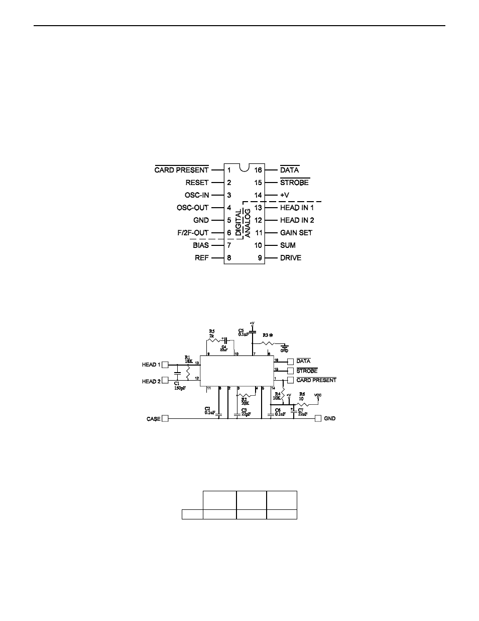
Connection Diagram (Pin Outs)
Recommended Circuit
This circuit is intended for use in systems employing F/2F data such as ID cards that conform to ISO 7811-2 or 7811-6.
21006516
VCC May be +2.7V to +5.5V
Tolerances: Resistors
±5%; C1, C3 ±5% NPO; other capacitors non-critical.
* R3 has different values for Rev B and Rev G. The table bellow shows the value of R3.
Table 2: Value of R3.
Rev
B
Rev
G
Rev
H
R3 470K 1.5M 1.5M
Printed Circuit Board Layout Requirements
The I.C. is a combined digital and analog system. The analog signal pins are very low level. Good layout practice
requires that there be a separation of head and other analog signals from the digital outputs. The digital signals are:
DATA, STROBE, CARD PRESENT, F/2F OUT, OSC-OUT and OSC-IN. The analog signals in order of sensitivity are
HEAD in 1&2, SUM, DRIVE, GSR and BIAS. The digital signals must not pass near the first four analog signals. The
layout below illustrates the requirements.
