Aiwa CDC-Z107 User Manual
Page 30
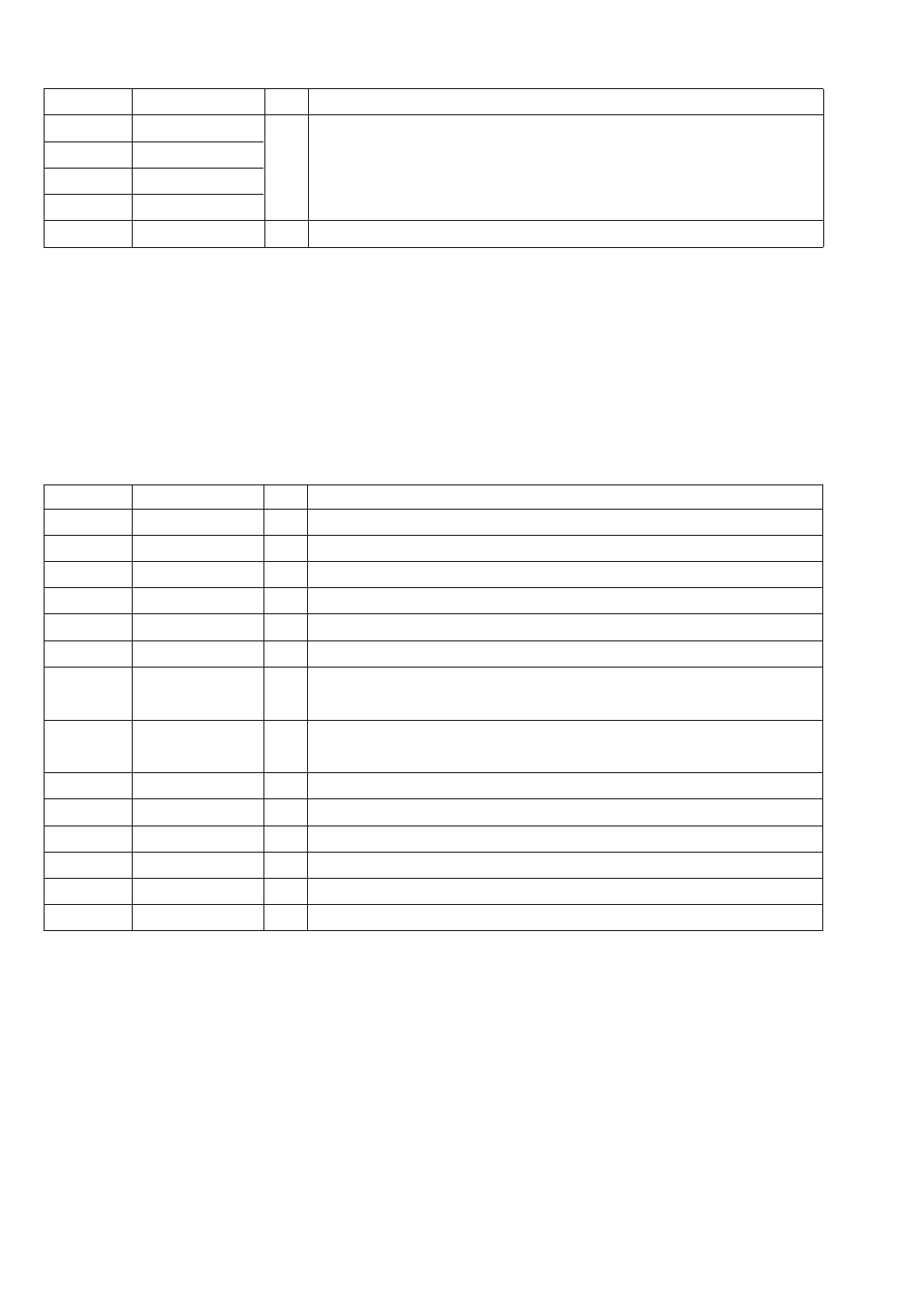
40
TP(R)
41
TUN(R)
I
Signal input pins.
42
CD(R)
43
AUX(R)
44
RSELO
O
Input selector output pin.
Pin No.
Pin Name
I/O
Description
Pin No.
Pin Name
I/O
Description
1 ~ 40
S1 ~ S40
O
LCD segment output.
41 ~ 43
COM1~ COM3
O
LCD command driver outputs.
44 ~ 49
KS1 ~ KS6
O
Key scan outputs.
50 ~ 54
KI1 ~ KI5
I
Key scan inputs. These pins have build-in pull-down resistor.
55
TEST
-
Test pin. (Connected to GND.)
56
VDD
-
Power supply.
57
VDD1
I
Used for applying the LCD drive 2/3 bias voltage externally. (Must be connected to
VDD2 when a 1/2 bias drive scheme is used.)
58
VDD2
I
Used for applying the LCD drive 1/3 bias voltage externally. (Must be connected to
VDD1 when a 1/2 bias drive scheme is used.
59
VSS
-
Power supply. (Connected to GND.)
60
OSC
I/O
Resistor and capacitor are attached externally form an oscillator circuit.
61
DO
O
Serial data interface pin; output data.
62
CE
O
Serial data interface pin; chip enable.
63
CL
O
Serial data interface pin; synchronization.
64
DI
O
Serial data interface pin; data transferred.
IC, LC75853NW
- 30 -