Access PCI-DIO-24D(H) User Manual
Page 22

Manual PCI-DIO-24DH
22
Programming the 8254
The counters are programmed by writing a control byte into the counter control register. Refer to the
previous register map for the base addresses of the counters and the counter control register. The control
byte specifies the counter to be programmed, the counter mode, the type of read/write operation, and the
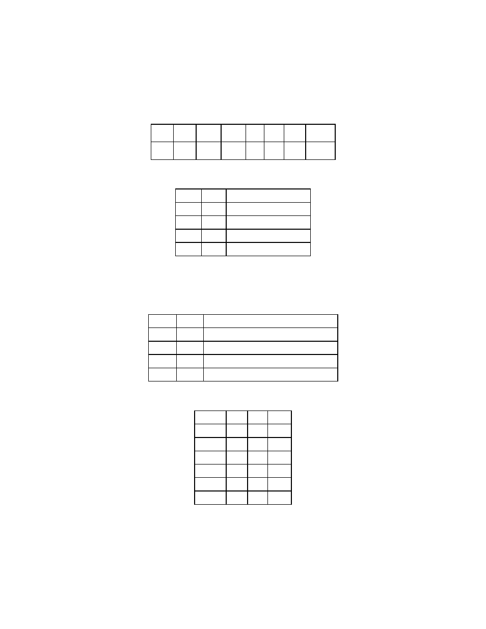
modulus. The control byte format is as follows:
B7
B6
B5
B4
B3
B2
B1
B0
SC1 SC0 RW1 RW0 M2 M1
M0 BCD
SC0-SC1: These bits select the counter that the control byte is destined for.
SC1 SC0 Function
0
0
Program Counter #0
0
1
Program Counter #1
1
0
Program Counter #2
1
1
Read/Write Cmd.*
* See section on Reading and Loading the Counters.
RW0-RW1: These bits select the read/write mode of the selected counter.
RW1 RW0 Counter Read/Write Function
0
0
Counter Latch Command
0
1
Read/Write LS Byte
1
0
Read/Write MS Byte
1
1
Read/Write LS Byte, then MS Byte
M0-M2: These bits set the operational mode of the selected counter.
Mode
M2 M1 M0
0
0
0
0
1
0
0
1
2
X
1
0
3
X
1
1
4
1
0
0
5
1
0
1
BCD: Set the selected counter to count in binary (BCD = 0) or BCD (BCD = 1).
