Figure 47. input stage overload recovery time, Figure 50. cmrr vs. frequency, Figure 48. output stage overload recovery time – Analog Devices AD602 User Manual
Page 19: Figure 51. psrr vs. frequency, Figure 49. transient response minimum gain
AD600/AD602
10
90
100
0%
50mV
5V
100nS
OUTPUT
INPUT
Figure 44. Gating Feedthrough to
Output, Gating Off to On
10
90
100
0%
500mV
1V
200nS
OUTPUT
INPUT
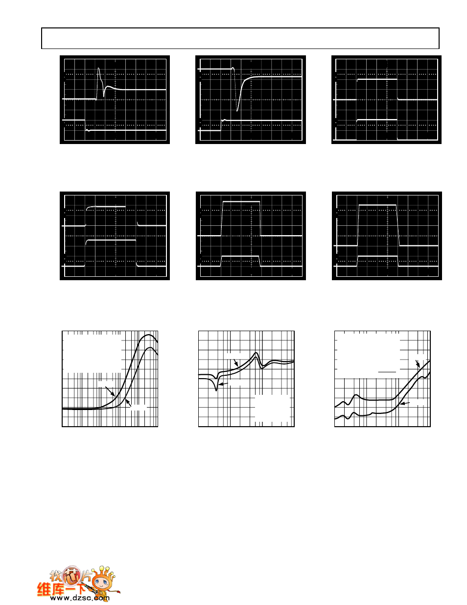
Figure 47. Input Stage Overload
Recovery Time
+10
1k
–15
–40
10k
100k
1M
10M
100M
–10
–5
0
+5
–35
–30
–25
–20
CMRR – dB
AD602
AD600
AD600:
AD602:
BOTH:
G=20dB
G=10dB
V =100mV RMS
V =
±
5V
R =500
Ω
T =25
°
C
CM
S
L
A
FREQUENCY — Hz
Figure 50. CMRR vs. Frequency
10
90
100
0%
50mV
5V
100nS
OUTPUT
INPUT
Figure 45. Gating Feedthrough to
Output, Gating On to Off
10
90
100
0%
200mV
1V
500nS
OUTPUT
INPUT
Figure 48. Output Stage Overload
Recovery Time
100k
1M
100M
10M
+20
–30
–80
+10
0
–10
–20
–40
–50
–60
–70
FREQUENCY – Hz
PSRR – dB
AD600
AD602
AD600: G=40dB
AD602: G=30dB
BOTH: R =500
Ω
V =0V
R =50
Ω
L
IN
S
Figure 51. PSRR vs. Frequency
10
90
100
0%
100mV
1V
500nS
OUTPUT
INPUT
Figure 46. Transient Response,
Medium and High Gain
10
90
100
0%
500mV
1V
500nS
OUTPUT
INPUT
Figure 49. Transient Response
Minimum Gain
100k
1M
100M
10M
–30
–80
+10
0
–10
–20
–40
–50
–60
–70
FREQUENCY – Hz
CROSSTALK – dB
AD600
AD602
AD600:
AD602:
BOTH:
CROSSTALK=20log
{ }
–90
CH1 G=40dB, V =0
CH2 G=20dB, V =100mV
CH1 G=30dB, V =0
CH2 G=10dB, V =316mV
V =1V RMS, R =50
Ω
,
R =500
Ω
IN
IN
OUT
S
L
CH1 V
CH2 V
OUT
IN
IN
IN
Figure 52. Crosstalk Between A1
and A2 vs. Frequency
–19–
REV. A