Analog Devices AD602 User Manual
Analog Devices Hobs

REV. A
Information furnished by Analog Devices is believed to be accurate and
reliable. However, no responsibility is assumed by Analog Devices for its
use, nor for any infringements of patents or other rights of third parties
which may result from its use. No license is granted by implication or
otherwise under any patent or patent rights of Analog Devices.
a
Dual, Low Noise, Wideband
Variable Gain Amplifiers
AD600/AD602*
One Technology Way, P.O. Box 9106, Norwood, MA 02062-9106, U.S.A.
Tel: 617/329-4700
Fax: 617/326-8703
FEATURES
Two Channels with Independent Gain Control
“Linear in dB” Gain Response
Two Gain Ranges:
AD600: 0 dB to +40 dB
AD602: –10 dB to +30 dB
Accurate Absolute Gain:
؎0.3 dB
Low Input Noise: 1.4 nV/
√
Hz
Low Distortion: –60 dBc THD at
؎1 V Output
High Bandwidth: DC to 35 MHz (–3 dB)
Stable Group Delay:
؎2 ns
Low Power: 125 mW (max) per Amplifier
Signal Gating Function for Each Amplifier
Drives High Speed A/D Converters
MIL-STD-883 Compliant and DESC Versions Available
APPLICATIONS
Ultrasound and Sonar Time-Gain Control
High Performance Audio and RF AGC Systems
Signal Measurement
PRODUCT DESCRIPTION
The AD600 and AD602 dual channel, low noise variable gain
amplifiers are optimized for use in ultrasound imaging systems,
but are applicable to any application requiring very precise gain,
low noise and distortion, and wide bandwidth. Each indepen-
dent channel provides a gain of 0 dB to +40 dB in the AD600
and –10 dB to +30 dB in the AD602. The lower gain of the
AD602 results in an improved signal-to-noise ratio at the out-
put. However, both products have the same 1.4 nV/
√
Hz
input
noise spectral density. The decibel gain is directly proportional
to the control voltage, is accurately calibrated, and is supply-
and temperature-stable.
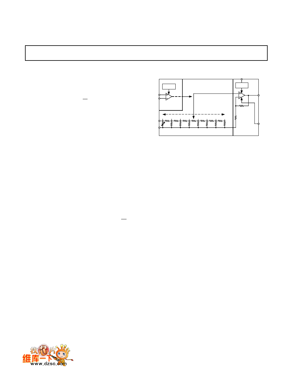
To achieve the difficult performance objectives, a proprietary
circuit form—the X-AMP®—has been developed. Each channel
of the X-AMP comprises a variable attenuator of 0 dB to
–42.14 dB followed by a high speed fixed gain amplifier. In this
way, the amplifier never has to cope with large inputs, and can
benefit from the use of negative feedback to precisely define the
gain and dynamics. The attenuator is realized as a seven-stage
R-2R ladder network having an input resistance of 100
Ω
, laser-
trimmed to
±
2%. The attenuation between tap points is 6.02 dB;
the gain-control circuit provides continuous interpolation be-
tween these taps. The resulting control function is linear in dB.
X-AMP is a registered trademark of Analog Devices, Inc.
*Patented.
The gain-control interfaces are fully differential, providing an
input resistance of ~15 M
Ω
and a scale factor of 32 dB/V (that
is, 31.25 mV/dB) defined by an internal voltage reference. The
response time of this interface is less than 1
µ
s. Each channel
also has an independent gating facility that optionally blocks sig-
nal transmission and sets the dc output level to within a few mil-
livolts of the output ground. The gating control input is TTL
and CMOS compatible.
The maximum gain of the AD600 is 41.07 dB, and that of the
AD602 is 31.07 dB; the –3 dB bandwidth of both models is
nominally 35 MHz, essentially independent of the gain. The
signal-to-noise ratio (SNR) for a 1 V rms output and a 1 MHz
noise bandwidth is typically 76 dB for the AD600 and 86 dB for
the AD602. The amplitude response is flat within
±
0.5 dB from
100 kHz to 10 MHz; over this frequency range the group delay
varies by less than
±
2 ns at all gain settings.
Each amplifier channel can drive 100
Ω
load impedances with
low distortion. For example, the peak specified output is
±
2.5 V
minimum into a 500
Ω
load, or
±
1 V into a 100
Ω
load. For a
200
Ω
load in shunt with 5 pF, the total harmonic distortion for
a
±
1 V sinusoidal output at 10 MHz is typically –60 dBc.
The AD600J and AD602J are specified for operation from 0
°
C
to +70
°
C, and are available in both 16-pin plastic DIP (N) and
16-pin SOIC (R). The AD600A and AD602A are specified for
operation from –40
°
C to +85
°
C and are available in both 16-pin
cerdip (Q) and 16-pin SOIC (R).
The AD600S and AD602S are specified for operation from
–55
°
C to +125
°
C and are available in a 16-pin cerdip (Q) pack-
age and are MIL-STD-883 compliant. The AD600S and
AD602S are also available under DESC SMD 5962-94572.
FUNCTIONAL BLOCK DIAGRAM
GAIN CONTROL
INTERFACE
V
G
RF1
20
Ω
PRECISION PASSIVE
INPUT ATTENUATOR
FIXED GAIN
AMPLIFIER
RF2
2.24k
Ω
(AD600)
694
Ω
(AD602)
A1OP
A1CM
C1HI
C1LO
SCALING
REFERENCE
GATING
INTERFACE
GAT1
41.07dB (AD600)
31.07dB (AD602)
500
Ω
62.5
Ω
0dB
–6.02dB –12.04dB –18.06dB
–22.08dB –30.1dB –36.12dB –42.14dB
R – 2R LADDER NETWORK
A1HI
A1LO
