Figure 35. gain error vs. gain control voltage, Figure 41. input impedance vs. frequency, 2 v p-p, r – Analog Devices AD602 User Manual
Page 18: 500 ω
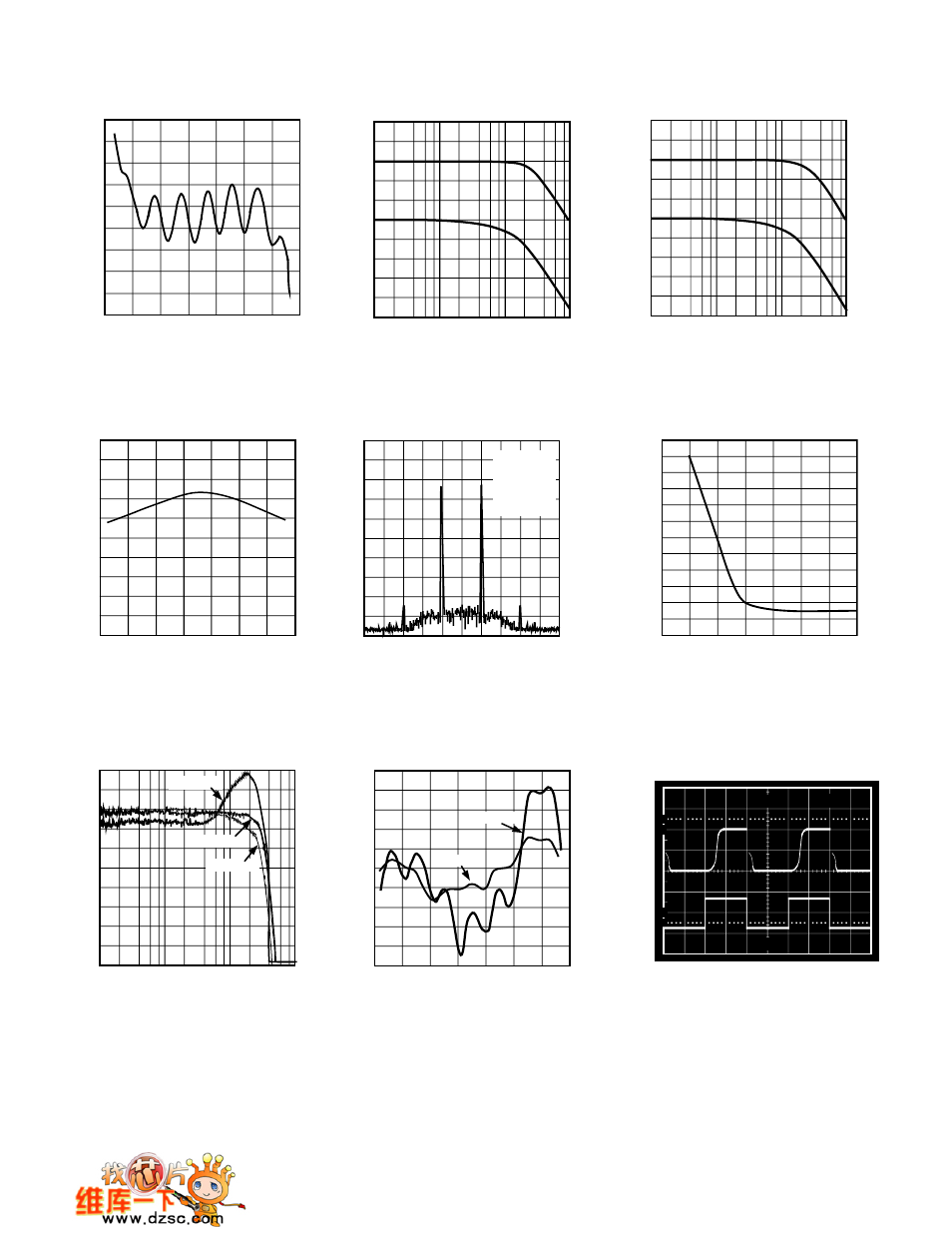
AD600/AD602–Typical Performance Characteristics
0.45
–0.45
0.7
–0.25
–0.35
–0.5
–0.7
–0.05
–0.15
0.05
0.15
0.25
0.35
0.5
0.3
0.1
–0.1
–0.3
GAIN CONTROL VOLTAGE – Volts
GAIN ERROR – dB
Figure 35. Gain Error vs. Gain
Control Voltage
10.0
9.0
8.0
–0.7
–0.5
0.7
0.5
0.3
0.1
–0.1
–0.3
9.8
9.6
9.4
9.2
8.2
8.8
8.6
8.4
GROUP DELAY – ns
GAIN CONTROL VOLTAGE – Volts
Figure 38. AD600 and AD602
Typical Group Delay vs. V
C
100k
1M
100M
10M
FREQUENCY – Hz
INPUT IMPEDANCE –
Ω
102
92
95
93
94
98
96
97
99
100
101
GAIN=40dB
GAIN=0dB
GAIN=20dB
Figure 41. Input Impedance vs.
Frequency
100k
1M
100M
10M
0
°
20dB
17dB
–45
°
–90
°
FREQUENCY – Hz
Figure 36. AD600 Frequency and
Phase Response vs. Gain
V =0V
10dB/DIV
CENTER
FREQ 1MHz
10kHz/DIV
G
Figure 39. Third Order Intermodula-
tion Distortion, V
OUT
= 2 V p-p,
R
L
= 500
Ω
6
–4
0.7
–1
–3
–0.5
–2
–0.7
2
0
1
3
4
5
0.5
0.1
0.3
–0.3
–0.1
GAIN CONTROL VOLTAGE – Volts
OUTPUT OFFSET VOLTAGE – mV
AD600
AD602
Figure 42. Output Offset vs. Gain
Control Voltage (Control Channel
Feedthrough)
100k
1M
100M
10M
0
°
10dB
7dB
–45
°
–90
°
FREQUENCY – Hz
Figure 37. AD602 Frequency and
Phase Response vs. Gain
–1.0
–3.4
–2.8
–3.2
50
–3.0
0
–2.2
–2.6
–2.4
–2.0
–1.8
–1.6
–1.2
–1.4
2000
1000
500
200
100
LOAD RESISTANCE –
Ω
NEGATIVE OUTPUT VOLTAGE LIMIT – Volts
Figure 40. Typical Output Voltage
vs. Load Resistance (Negative Out-
put Swing Limits First)
10
90
100
0%
1V VOUT
1V VC
1
µ
S
OUTPUT
INPUT
Figure 43. Gain Control Channel
Response Time. Top: Output Volt-
age, 2 V max, Bottom: Gain Con-
trol Voltage V
C
=
±
625 mV
REV. A
–18–