SENA Parani-BCD100 User Manual
Page 6
PARANI-BCD100
Page 6 of 22
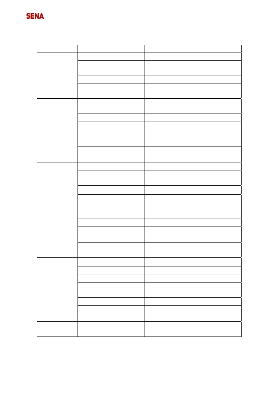
1.5 Pin Descriptions
Table 1-1 Pin descriptions
Function
Pin Name
Pin Number
Description
USB Interface
USB_DP
11
USB data plus
USB_DN
10
USB data minus
UART Interface
UART_TXD
8
UART data output
UART_RXD
7
UART data input
UART_RTS
6
UART request to send active low
UART_CTS
9
UART clear to send active low
PCM Interface
PCM_OUT 15
Synchronous
data
output
PCM_IN 12
Synchronous
data
input
PCM_SYNC 13 Synchronous
data
sync
PCM_CLK 14
Synchronous
data
clock
SPI Interface
SPI_MISO
20
SPI data output
SPI_MOSI
23
SPI data input
SPI_CSB
22
Chip select for SPI, active low
SPI_CLK 21
SPI
clock
PIO Interface
PIO_2
29
Programmable input/output line
PIO_3
28
Programmable input/output line
PIO_4
24
Programmable input/output line
PIO_5
25
Programmable input/output line
PIO_6
26
Programmable input/output line
PIO_7
27
Programmable input/output line
PIO_8
30
Programmable input/output line
PIO_9
31
Programmable input/output line
PIO_10
32
Programmable input/output line
PIO_11
33
Programmable input/output line
AIO_0
4
Analogue programmable input/output line
AIO_1
5
Analogue programmable input/output line
Power
PVCC
3
Power supply for power amplifier, 3.3V
+3V3
16
Power supply for system, 3.3V
GND 1
Ground
GND 2
Ground
GND 17
Ground
GND 19
Ground
GND 34
Ground
GND 35
Ground
Others
RF_I/O
36
Transmitter output/receiver input
RESETB
18
Reset, active low, > 5ms to cause a reset