Bottom termination soldering techniques (cont.) – Ironwood Electronics Bottom Termination Soldering Techniques User Manual
Page 2
Page 2 of 2
Bottom Termination Soldering Techniques (cont.)
Tel: (800) 404-0204
www.ironwoodelectronics.com
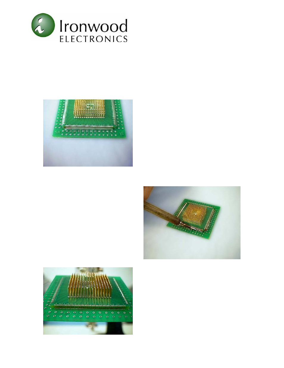
(4) Apply a generous amount of flux along the side of the adapter PCB as shown in
Figure 4.
(5) Using a very fine tipped soldering iron (spade tip 0.03" diameter and 60
° chisel
angle), add solder to the soldering tip using solder wire (low temp, 63Sn/37Pb) to form a
blob of solder approximately 1/8" diameter on its tip. Use a microscope or magnifying
lens, if available, to view the process while
soldering.
(6) Start at one corner and pull the tip of the
soldering iron along the side of the foot as
shown in Figure 5. Continue down the side of
the foot until a suitable fillet is present
between
all adapter pads and target PCB pads.
(7) Repeat this step for the remaining three
sides of the adapter. Caution must be used
when touching the soldering iron tip to the
emulator foot. Excessive heat or pressure
may damage the pads on the adapter or on
the target PCB.
(8) Clean thoroughly in an ultra-sonic
cleaner. The picture of the solder
connection is shown
in Figure 6.
The adapter is similar to discrete chip
components, leadless chip carriers, and
other devices that have metalized
terminations on the bottom side only. The
solder joints produced by the above process
are acceptable under class 1 and 2 of IPC-A-
610B, Section 10. 2. 1, Chip
Components/Bottom only Terminations
standard.
filename: KSI.doc, Rev A
Figure 4: Applying Flux
Figure 5: Soldering Process
Figure 6: Solder Connections