Rainbow Electronics MAX5095A User Manual
Page 13
V
CC
and Startup
In normal operation, V
CC
is derived from a tertiary wind-
ing of the transformer. However, at startup there is no
energy delivered through the transformer, thus a resistor
must be connected from V
CC
to the input power source
(see R
ST
and C
ST
in Figures 5 to 8). During startup, C
ST
charges up through R
ST
. The 5V reference generator,
comparator, error amplifier, oscillator, and drive circuit
remain off during UVLO to reduce startup current below
65µA. When V
CC
reaches the undervoltage-lockout
threshold of 8.4V, the output driver begins to switch and
the tertiary winding supplies power to V
CC
. V
CC
has an
internal 26.5V current-limited clamp at its input to protect
the device from overvoltage during startup.
Size the startup resistor, R
ST
, to supply both the maxi-
mum startup bias (I
START
) of the device (65µA max)
and the charging current for C
ST
. The startup capacitor
C
ST
must charge to 8.4V within the desired time period
t
ST
(for example, 500ms). The size of the startup
capacitor depends on:
1) IC operating supply current at a programmed oscilla-
tor frequency (f
OSC
).
2) The time required for the bias voltage, derived from
a bias winding, to go from 0 to 9V.
3) The MOSFET total gate charge.
4) The operating frequency of the converter (f
SW
).
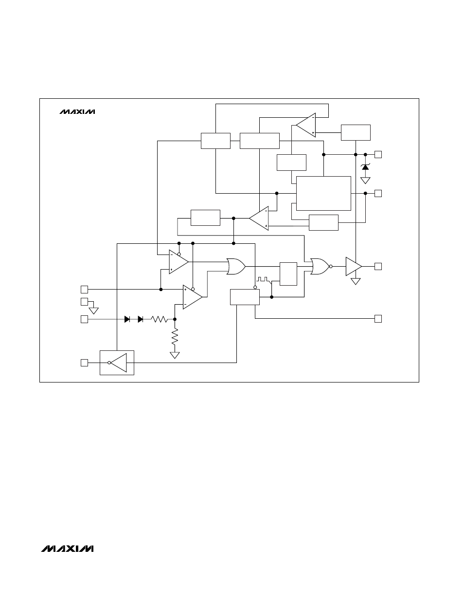
MAX5094A/B/C/D/MAX5095A/B/C
High-Performance, Single-Ended, Current-Mode
PWM Controllers
______________________________________________________________________________________
13
UVLO
REFERENCE
2.5V
PREREGULATOR
5V
VOLTAGE-
DIVIDER
THERMAL
SHUTDOWN
EN-REF
BG
SNS
V
DD
5V REGULATOR
VOLTAGE-
DIVIDER
8
7
26.5V
V
CC
REF
2.5V
VP
REG_OK
DELAY
S
R
Q
OSC
Q
4 R
T
/C
T
6 OUT
ILIM
CPWM
0.3V
EN-DRV-BAR
R
2R
3
5
1
2
CS
GND
COMP
ADV_CLK
CLK
MAX5095C
VP
2.5V
50% MAX DUTY CYCLE
8.4V/7.6V
Figure 3. MAX5095C Functional Diagram