Rainbow Electronics MAX1627 User Manual
Page 2
MAX1626/MAX1627
5V/3.3V or Adjustable, 100% Duty-Cycle,
High-Efficiency, Step-Down DC-DC Controllers
2
_______________________________________________________________________________________
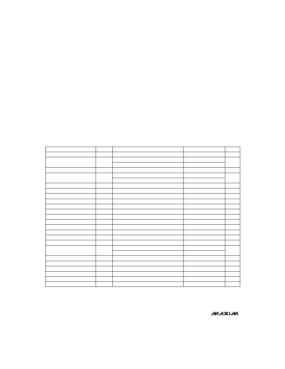
ABSOLUTE MAXIMUM RATINGS
ELECTRICAL CHARACTERISTICS
(V+ = +3V to +16.5V, SHDN =
3/5 = 0V, T
A
= 0°C to +85°C, unless otherwise noted.)
Stresses beyond those listed under “Absolute Maximum Ratings” may cause permanent damage to the device. These are stress ratings only, and functional
operation of the device at these or any other conditions beyond those indicated in the operational sections of the specifications is not implied. Exposure to
absolute maximum rating conditions for extended periods may affect device reliability.
Supply Voltage, V+ to GND.......................................-0.3V, +17V
OUT, FB,
3/5, SHDN, REF, CS, EXT to GND ...-0.3V, (V+ + 0.3V)
Maximum Current at REF (I
REF
) ..........................................15mA
Maximum Current at EXT (I
EXT
) ..........................................50mA
Continuous Power Dissipation (T
A
= +70°C)
SO (derate 5.88mW/°C above +70°C) ..........................471mW
Operating Temperature Range
MAX1626ESA/MAX1627ESA ............................-40°C to +85°C
Storage Temperature Range .............................-65°C to +160°C
Lead Temperature (soldering, 10sec) .............................+300°C
0µA
≤
I
REF
≤
100µA
I
LOAD
= 0µA
30mA < I
LOAD
< 2.0A, V+ = 8V
V+ = SHDN = 16.5V (shutdown)
6.0V < V+ < 12.0V, I
LOAD
= 1A
Operating, no load
Output in regulation
Output forced to 0V
V+ = 5V
3/5 = 0V or V+
MAX1627
Circuit of Figure 1,
3/5 = V+ (Note 1)
MAX1626,
3/5 = V+, output forced to 5V
SHDN = 0V or V+
MAX1627, includes hysteresis
CONDITIONS
mV
4
10
REF Load Regulation
V
1.27
1.30
1.33
V
REF
Reference Voltage
mV/A
15
Load Regulation
mV/V
5
Line Regulation
%
100
EXT Duty-Cycle Limit
µs
1.5
2.0
2.5
8
10
12
Minimum EXT Off Time
Ω
10
EXT Resistance
µA
±1
3/5 Leakage Current
V
0.5
3/5 Input Voltage Low
V
V+ - 0.5
3/5 Input Voltage High
µA
±1
SHDN Input Current
V
0.4
SHDN Input Voltage Low
µA
1
I+
Supply Current into V+
70
90
V
3.0
16.5
V+
Input Voltage Range
V
1.6
SHDN Input Voltage High
mV
85
100
115
V
CS
CS Threshold Voltage
µA
0
10
CS Input Current
nA
0
35
FB Leakage Current
V
2.7
2.8
Undervoltage Lockout
4.85
5.00
5.15
µA
24
37
50
I
OUT
OUT Input Current
V
1.27
1.30
1.33
FB Threshold Voltage
UNITS
MIN
TYP
MAX
SYMBOL
PARAMETER
V+ = 3V to 16.5V, I
LOAD
= 0µA
µV/V
10
100
REF Line Regulation
Circuit of Figure 1,
3/5 = 0V (Note 1)
V
3.20
3.30
3.40
V
OUT
Output Voltage