Rainbow Electronics MAX1627 User Manual
Page 12

MAX1626/MAX1627
current feedback signal and causing jitter. 0.47µF is
recommended. Increase the value as necessary in
high-power applications.
Bypass REF with 0.1µF. This capacitor should be
placed within 0.2 inches (5mm) of the IC, next to REF,
with a direct trace to GND (Figure 7).
Layout Considerations
High-frequency switching regulators are sensitive to PC
board layout. Poor layout introduces switching noise into
the current and voltage feedback signals, resulting in jit-
ter, instability, or degraded performance. The current-
sense resistor must be placed within 0.2 inches (5mm)
of the controller IC, directly between V+ and CS. Place
voltage feedback resistors (MAX1627) next to the FB pin
(no more than 0.2") rather than near the output. Place
the 0.47µF input and 0.1µF reference bypass capacitors
within 0.2 inches (5mm) of V+ and REF, and route
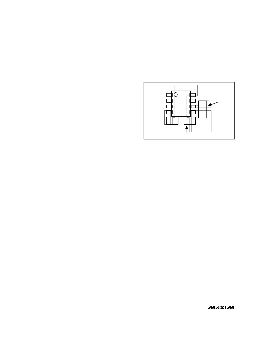
directly to GND. Figure 7 shows the recommended lay-
out and routing for these components.
High-power traces, highlighted in the
Typical Operating
Circuit (Figure 1), should be as short and as wide as
possible. The supply-current loop (formed by C2, C3,
R
SENSE
, U1, L1, and C1) and commutation-current loop
(D1, L1, and C1) should be as tight as possible to
reduce radiated noise. Place the anode of the commuta-
tion diode (D1) and the ground pins of the input and
output filter capacitors close together, and route them to
a common “star-ground” point. Place components and
route ground paths so as to prevent high currents from
causing large voltage gradients between the ground pin
of the output filter capacitor, the controller IC, and the
reference bypass capacitor. Keep the extra copper on
the component and solder sides of the PC board, rather
than etching it away, and connect it to ground for use as
a pseudo-ground plane. Refer to the MAX1626
Evaluation Kit manual for a two-layer PC board example.
Stability and MAX1627 Feedback
Compensation
Use proper PC board layout and recommended exter-
nal components to ensure stable operation. In one-
shot, sequenced PFM DC-DC converters, instability is
manifested as “Motorboat Instability.” It is usually
caused by excessive noise on the current or voltage
feedback signals, ground, or reference, due to poor PC
board design or external component selection.
Motorboat instability is characterized by grouped
switching pulses with large gaps and excessive low-
frequency output ripple. It is normal to see some
grouped switching pulses during the transition from
discontinuous to continuous current mode. This effect
is associated with small gaps between pulse groups
and output ripple similar to or less than that seen dur-
ing no-load conditions.
Instability can also be caused by excessive stray capaci-
tance on FB when using the MAX1627. Compensate for
this by adding a 0pF to 330pF feed-forward capacitor
across the upper feedback resistor (R2 in Figure 5).
MAX1626/MAX1627 vs.
MAX1649/MAX1651 vs.
MAX649/MAX651
The MAX1626/MAX1627 are specialized, third-genera-
tion upgrades to the MAX649/MAX651 step-down con-
trollers. They feature improved efficiency, a reduced
current-sense threshold (100mV), soft-start, and a
100% duty cycle for lowest dropout. The MAX649/
MAX651 have a two-step (210mV/110mV) current-
sense threshold. The MAX1649/MAX1651 are second-
generation upgrades with a 96.5% maximum duty cycle
for improved dropout performance and a reduced cur-
rent-sense threshold (110mV) for higher efficiency,
especially at low input voltages. The MAX1649/
MAX1651 are preferable for special applications where
a 100% duty cycle is undesirable, such as flyback and
SEPIC circuits.
Since the MAX1626’s pinout is similar to those of the
MAX649 and MAX1649 family parts, the MAX1626 can
be substituted (with minor external component value
changes) into fixed-output mode applications, provided
the PC board layout is adequate. The MAX1627 can
also be substituted when MAX649 or MAX1649 family
parts are used in adjustable mode, but the feedback
resistor values must be changed, since the MAX1627
has a lower reference voltage (1.3V vs. 1.5V). Reduce
the current-sense resistor value by 50% when substitut-
ing for the MAX649 or MAX651.
5V/3.3V or Adjustable, 100% Duty-Cycle,
High-Efficiency, Step-Down DC-DC Controllers
12
______________________________________________________________________________________
MAX1626
yyyyy
yyyyy
yyyyy
yyyyy
yyyyy
yyyyy
yyyyy
yyyyy
yyyyy
yyyy
yyyy
yyyy
yyyy
yyyy
yyyy
yyyy
yy
yy
yy
C
REF
C
V+ BYPASS
4x
SCALE
R
SENSE
Figure 7. Recommended Placement and Routing of the
Current-Sense Resistor, 0.1µF Reference, and 0.47µF Input
Bypass Capacitors
