Rainbow Electronics MAX1686H User Manual
Page 5
MAX1686/MAX1686H
3V to 5V Regulating
Charge Pumps for SIM Cards
_______________________________________________________________________________________
5
NAME
FUNCTION
1
3/5
3V/5V Select Input. When low, the output is regulated at 4.75V for MAX1686, 5.00V for MAX1686H. When
high, the output is shorted to the input.
2
SHDN
Active-Low Shutdown Input. SHDN = GND is off. Output is actively pulled low in shutdown.
PIN
3
IN
Supply Input Pin. Can range from 2.7V to 4.2V. Bypass to ground with a ceramic capacitor.
4
GND
Ground Pin
8
OUT
Power Output. Bypass to GND with an output filter capacitor.
7
CXP
Positive Terminal of the Charge-Pump Transfer Capacitor
6
CXN
Negative Terminal of the Charge-Pump Transfer Capacitor
5
PGND
Power Ground. Connect to GND through a short trace.
Pin Description
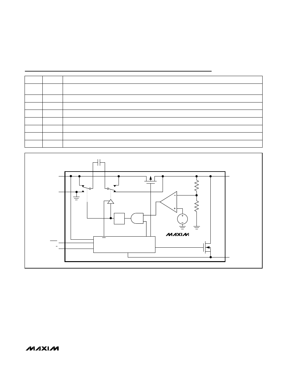
_______________Detailed Description
The MAX1686/MAX1686H charge pumps provide two
modes of operation: 3V mode or 5V mode. The devices
consist of an error amplifier, a 1.23V bandgap refer-
ence, an internal resistive feedback network, a 1MHz
oscillator, high-current MOSFET drivers and switches,
and a power-management block as shown in the
Functional Diagram
(Figure 1). In 3V mode (3/5 = IN),
the input is connected to the output through a 2.5
Ω
switch. In 5V mode (3/5 = GND), the MAX1686’s output
voltage is regulated at 4.75V (5.00V for the MAX1686H)
with a 2.7V to 4.2V input and can deliver more than
12mA of load current.
Designed specifically for compact applications, these
regulators require only three small external capacitors.
The Skip Mode control scheme provides high efficiency
over a wide output current range. The devices offer a
shutdown feature which actively discharges the output
to ground and reduces the supply current to less than
MAX1686
MAX1686H
C
X
POWER
MANAGEMENT
DIS
SS
OSC
CXP
CXN
EN
SHDN
3/5
1.23V
GND
PGND
IN
S1
S2
PWROK
OUT
Figure 1. Functional Diagram