Rainbow Electronics MAX1686H User Manual
Page 2
MAX1686/MAX1686H
3V to 5V Regulating
Charge Pumps for SIM Cards
2
_______________________________________________________________________________________
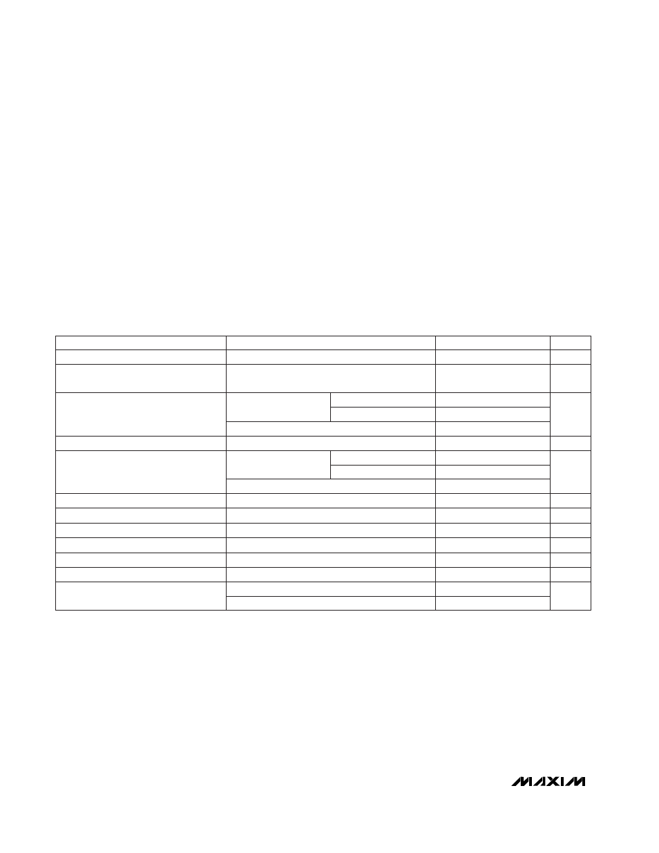
ABSOLUTE MAXIMUM RATINGS
ELECTRICAL CHARACTERISTICS
(V
IN
= V
SHDN
= 3.3V, 3/5 = GND, C
X
= 0.22µF, C
OUT
= 10µF (see
Applications Information
section to use smaller capacitors),
T
A
= T
MIN
to T
MAX
, unless otherwise noted. Typical values are at T
A
= +25°C.) (Note 1)
IN, OUT, SHDN, 3/5 to GND.....................................-0.3V to +6V
CXP to GND..............................................-0.3V to (V
OUT
+ 0.3V)
CXN to GND ................................................-0.3V to (V
IN
+ 0.3V)
PGND to GND ......................................................-0.3V to + 0.3V
OUT Short Circuit to GND ..........................................Continuous
IN-to-OUT Current...............................................................50mA
Continuous Power Dissipation (T
A
= +70°C )
8-Pin µMAX (derate 4.1mW/°C above +70°C) .............330mW
Operating Temperature Range
MAX1686EUA/MAX1686HEUA........................-40°C to +85°C
Junction Temperature ......................................................+150°C
Storage Temperature Range .............................-65°C to +165°C
Lead Temperature (soldering, 10sec) .............................+300°C
PARAMETER
CONDITIONS
MIN
TYP
MAX
UNITS
Input Voltage Range
2.7
4.2
V
Input Undervoltage-Lockout
Threshold Voltage
0.8
1.2
1.6
V
Quiescent Supply Current
Charge pump enabled,
no load, 3/5 = GND
µA
Charge pump disabled, no load, 3/5 = IN
Shutdown Supply Current
V
IN
= 3.6V, SHDN = GND
0.1
5
V
OUT Output Voltage
4.55
4.75
5.25
V
3/5
= V
IN
= 3.0V
2.5
5
Ω
OUT Short-Circuit Current
3/5 = GND or IN
20
100
200
mA
Logic Input Low Voltage
SHDN, 3/5
0.5
·
V
IN
0.3
·
V
IN
V
Logic Input High Voltage
SHDN, 3/5
0.7
·
V
IN
0.5
·
V
IN
V
Logic Input Leakage Current
SHDN, 3/5 = GND or IN
0.1
1
µA
4.75
5.00
5.25
OUT Discharge Switch On-Resistance
3/5 = GND or IN, SHDN = GND
80
200
Ω
IN-to-OUT Switch On-Resistance
T
A
= +25°C
800
1000
1200
µA
Note 1:
Electrical specifications are measured by pulse testing and are guaranteed for a junction temperature within the operating
temperature range, unless otherwise noted. Limits are 100% production tested at T
A
= +25°C. Limits over the entire operat-
ing temperature range are guaranteed through correlation using Statistical Quality Control (SQC) methods and are not pro-
duction tested.
Stresses beyond those listed under “Absolute Maximum Ratings” may cause permanent damage to the device. These are stress ratings only, and functional
operation of the device at these or any other conditions beyond those indicated in the operational sections of the specifications is not implied. Exposure to
absolute maximum rating conditions for extended periods may affect device reliability.
T
A
= +25°C
45
100
3
10
Charge-Pump Frequency
T
A
= -40°C to +85°C
700
1300
kHz
T
A
= -40°C to +85°C
150
3/5 = IN
V
IN
MAX1686
MAX1686H
V
IN
= 2.7V to 4.2V,
load = 0 to 12mA