Max2055, Chip information – Rainbow Electronics MAX2055 User Manual
Page 12
MAX2055
package. This pad should be connected to the ground
plane of the board by using multiple vias under the
device to provide the best RF/thermal conduction path.
Solder the exposed pad on the bottom of the device
package to a PC board exposed pad.
The MAX2055 Evaluation Kit can be used as a refer-
ence for board layout. Gerber files are available upon
request at www.maxim-ic.com.
Power-Supply Bypassing
Proper voltage-supply bypassing is essential for high-
frequency circuit stability. Bypass each V
CC
pin with a
1000pF and 100pF capacitor. Connect the 100pF
capacitor as close to the device as possible. Resistor
R7 helps reduce switching transients. If switching tran-
sients are not a concern, R7 is not required. Therefore,
connect pin 9 directly to V
CC
.
Exposed Paddle RF Thermal
Considerations
The EP of the MAX2055’s 20-pin TSSOP-EP package
provides a low thermal-resistance path to the die. It is
important that the PC board on which the IC is mounted
be designed to conduct heat from this contact. In addi-
tion, the EP provides a low-inductance RF ground path
for the device.
It is recommended that the EP be soldered to a ground
plane on the PC board, either directly or through an
array of plated via holes.
Soldering the pad to ground is also critical for efficient
heat transfer. Use a solid ground plane wherever
possible.
Digitally Controlled, Variable-Gain, Differential
ADC Driver/Amplifier
12
______________________________________________________________________________________
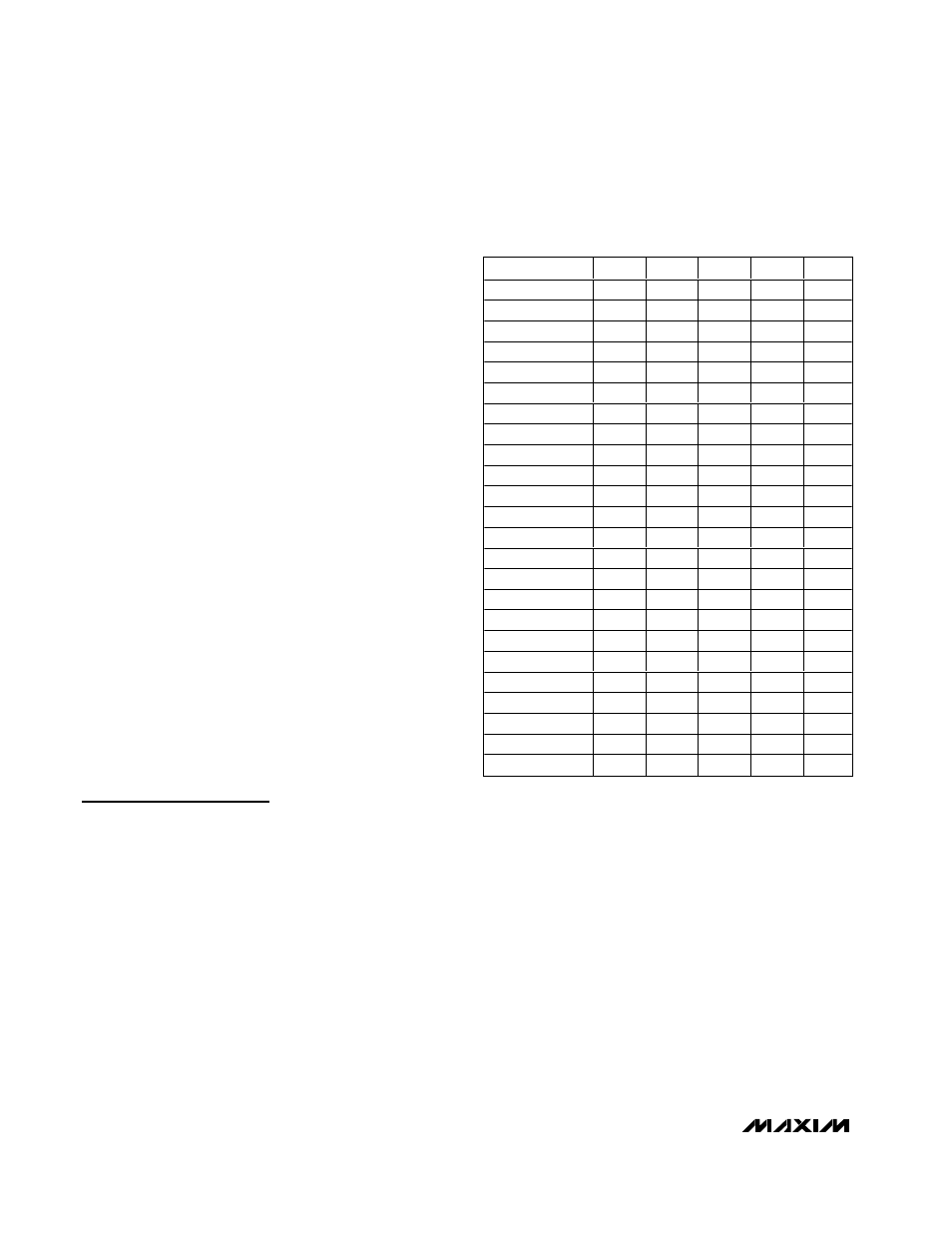
ATTENUATION
B4
B3*
B2
B1
B0
0
0
0
0
0
0
1
0
0
0
0
1
2
0
0
0
1
0
3
0
0
0
1
1
4
0
0
1
0
0
5
0
0
1
0
1
6
0
0
1
1
0
7
0
0
1
1
1
8
0
1
0
0
0
9
0
1
0
0
1
10
0
1
0
1
0
11
0
1
0
1
1
12
0
1
1
0
0
13
0
1
1
0
1
14
0
1
1
1
0
15
0
1
1
1
1
16
1
X
0
0
0
17
1
X
0
0
1
18
1
X
0
1
0
19
1
X
0
1
1
20
1
X
1
0
0
21
1
X
1
0
1
22
1
X
1
1
0
23
1
X
1
1
1
Table 3. Attenuation Setting vs. Gain-
Control Bits
*Enabling B4 disables B3 and the minimum attenuation is
16dB.
Chip Information
TRANSISTOR COUNT: 325
PROCESS: BiCMOS