Pin descriptions (continued) – Rainbow Electronics MAX542 User Manual
Page 6
MAX541/MAX542
+5V, Serial-Input, Voltage-Output, 16-Bit DACs
6
_______________________________________________________________________________________
________________________________________________Pin Descriptions (continued)
;;
;;
;;;;;;;;;
;;
;;
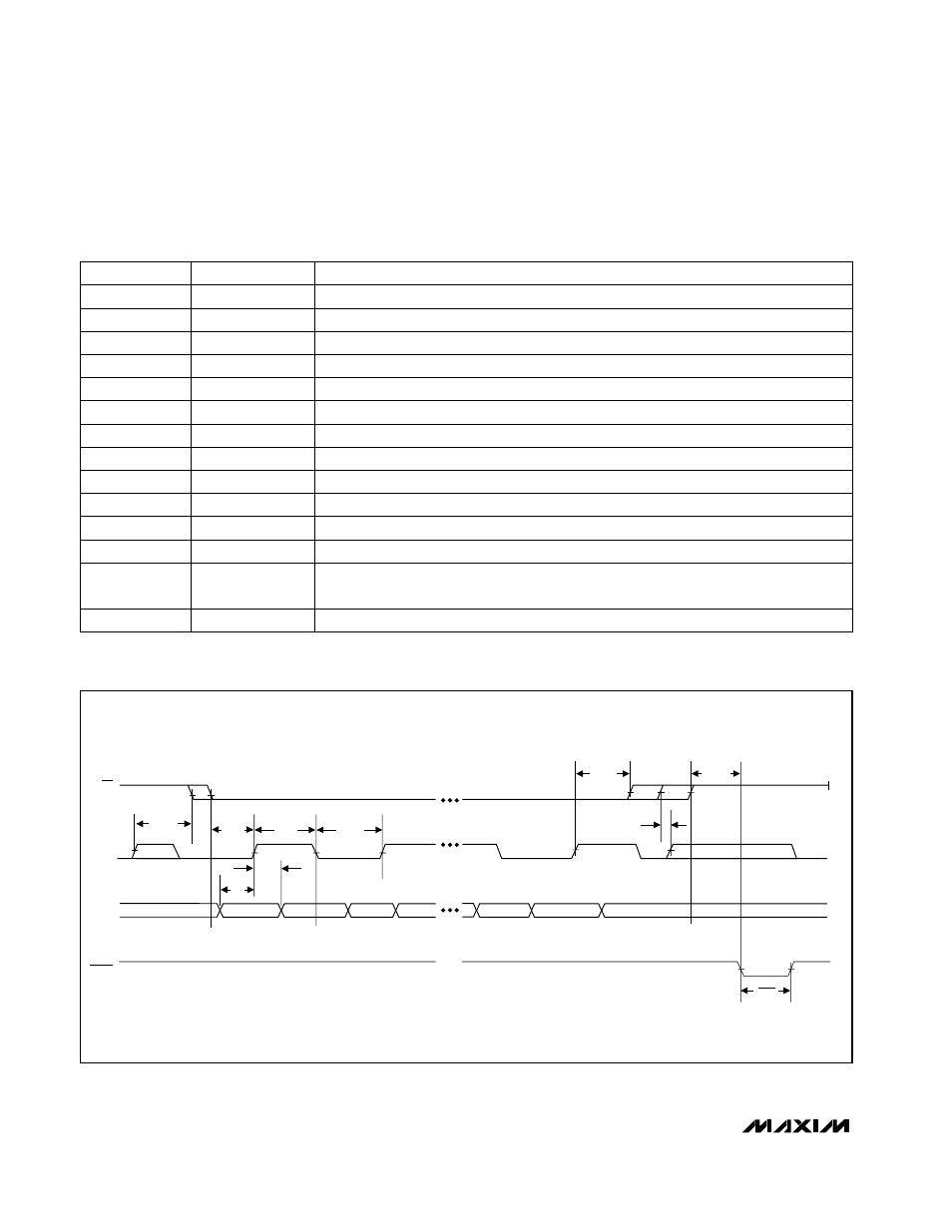
t
CSHO
t
CH
t
CSSO
t
CL
t
DH
t
DS
t
CSH1
t
CSS1
t
LDACS
t
LDAC
CS
SCLK
DIN
LDAC*
*MAX542 ONLY
D15
D14
D0
Figure 1. Timing Diagram
+5V Supply Voltage
V
DD
Digital Ground
DGND
12
LDAC Input. A falling edge updates the internal DAC latch.
LDAC
11
Serial Data Input
DIN
10
No Connection. Not internally connected.
N.C.
9
Serial Clock Input. Duty cycle must be between 40% and 60%.
SCLK
8
Chip-Select Input
CS
7
Voltage Reference Input (force). Connect REFF to external +2.5V reference.
REFF
6
Voltage Reference Input (sense). Connect REFS to external +2.5V reference.
REFS
5
Analog Ground (sense)
AGNDS
4
Analog Ground (force)
AGNDF
3
DAC Output Voltage
OUT
2
Feedback Resistor. Connect to external op amp’s output in bipolar mode.
RFB
1
FUNCTION
NAME
PIN
Junction of internal scaling resistors. Connect to external op amp’s inverting input in
bipolar mode.
INV
13
14
MAX542