Rainbow Electronics MAX101А User Manual
Page 2
MAX101A
500Msps, 8-Bit ADC with Track/Hold
2
_______________________________________________________________________________________
ABSOLUTE MAXIMUM RATINGS
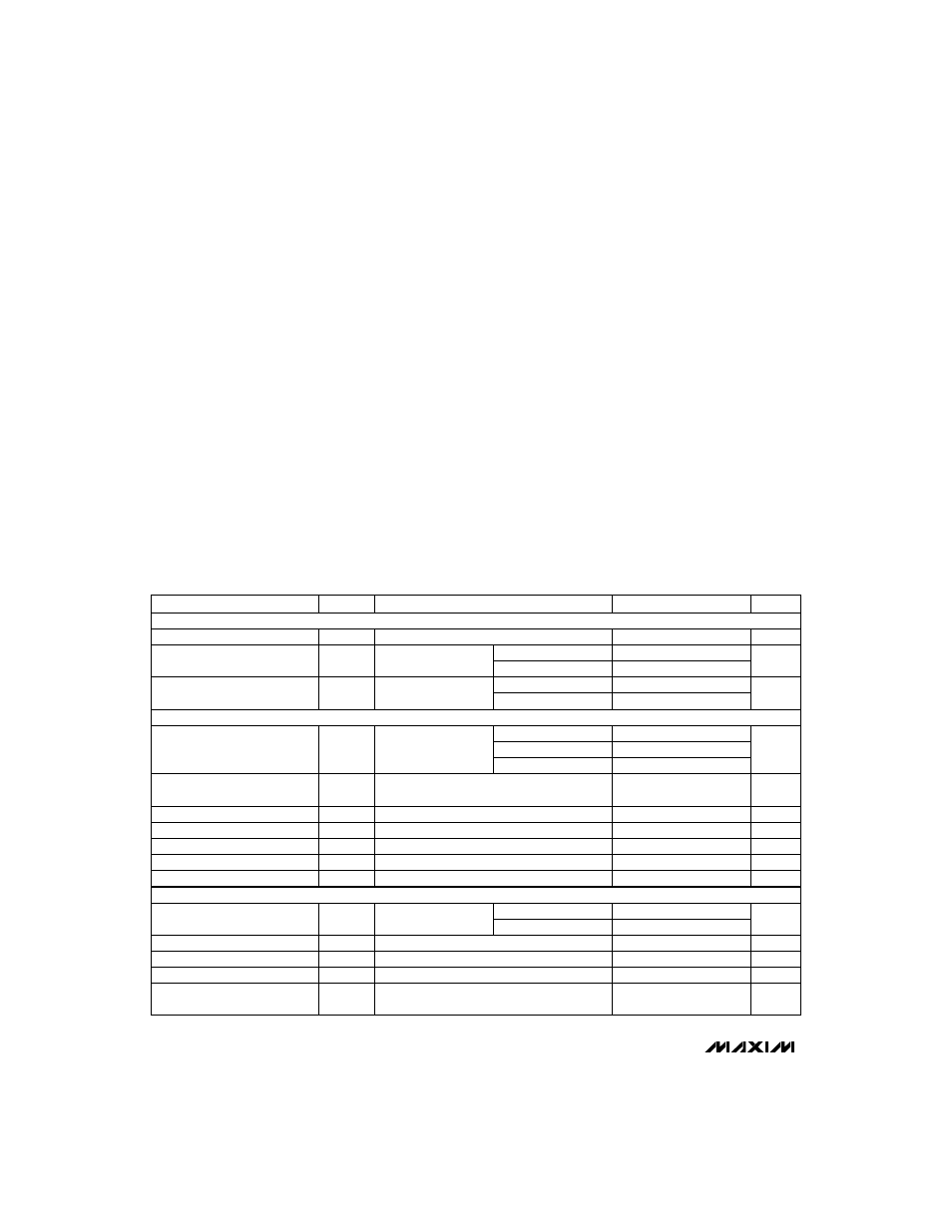
ELECTRICAL CHARACTERISTICS
(V
EE
= -5.2V, V
CC
= +5V, R
L
= 100
Ω
to -2V, VA
RT
, VB
RT
= 0.95V, VA
RB
, VB
RB
= -0.95V, T
A
= +25°C, unless otherwise noted.
T
MIN
to T
MAX
= 0°C to +70°C.) (Note 3)
Stresses beyond those listed under “Absolute Maximum Ratings” may cause permanent damage to the device. These are stress ratings only, and functional
operation of the device at these or any other conditions beyond those indicated in the operational sections of the specifications is not implied. Exposure to
absolute maximum rating conditions for extended periods may affect device reliability.
Supply Voltages (Note 1)
V
CC
...........................................................................0V to +7V
V
EE
.............................................................................-7V to 0V
V
CC
- V
EE
.........................................................................+12V
Analog Input Voltage .............................................................±2V
Reference Voltage (VA
RT
, VB
RT
)...........................-0.3V to +1.5V
Reference Voltage (VA
RB
, VB
RB
) ..........................-1.5V to +0.3V
Clock Input Voltage (V
IH
, V
IL
) .....................................-2.3V to 0V
DIV10 Input Voltage (V
IH
, V
IL
).......................................V
EE
to 0V
Output Current, (I
OUT(max)
)
T
J
<100°C .......................................................................14mA
100°C < T
J
<120°C.........................................................12mA
Operating Temperature Range...............................0°C to +70°C
Operating Junction Temperature (Note 2)............0°C to +120°C
Storage Temperature Range .............................-65°C to +150°C
Lead Temperature (soldering, 10sec) .............................+250°C
Full scale
AData, BData,
no missing codes
f
CLK
= 500MHz,
V
IN
= 95% full scale
(Note 5)
Bits
7.1
f
AIN
= 10MHz
f
AIN
= 125MHz
Zero scale
7.6
f
AIN
= 250MHz
AData, BData
6.7
7.0
ENOB
Effective Bits
CONDITIONS
Figure 4
Figure 4
(Note 7)
f
AIN
= 125MHz, f
CLK
= 500MHz,
V
IN
= 95% full scale (Note 6)
ps
2
t
AJ
ps
270
t
AW
Aperture Width
Aperture Jitter
205
290
Msps
500
f
CLK
Maximum Conversion Rate
dB
44.5
SNR
Signal-to-Noise Ratio
GHz
1.2
BW
3dB
Analog Input Bandwidth
AIN+ to AIN-, Table 2,
T
A
= T
MIN
to T
MAX
mV
-290
-205
V
IN
Input Voltage Range
AIN+, AIN-, to GND
T
A
= T
MIN
to T
MAX
±0.75
±0.50
T
A
= +25°C
T
A
= T
MIN
to T
MAX
Bits
8
Resolution
AIN+, AIN-, T
A
= T
MIN
to T
MAX
Ω
/°C
0.008
Input Resistance
Temperature Coefficient
LSB
±0.75
INL
Integral Nonlinearity (Note 4)
Ω
49
51
R
I
Input Resistance
mV
1.65
2.35
LSB
mV
-23
23
V
IO
Input Offset Voltage
UNITS
MIN
TYP
MAX
SYMBOL
PARAMETER
Least Significant Bit Size
T
A
= +25°C
T
A
= T
MIN
to T
MAX
LSB
±0.85
DNL
Differential Nonlinearity
Note 1:
The digital control inputs are diode protected. However, limited protection is provided on other pins. Permanent damage
may occur on unconnected units under high-energy electrostatic fields. Keep unused units in supplied conductive carrier or
shunt the terminals together.
Note 2:
Typical thermal resistance, junction-to-case R
θ
JC
= 5°C/W and thermal resistance, junction to ambient (MAX101ACFR)
R
θ
JA
=12°C/W, if 200 lineal ft/min airflow is provided. See
Package Information.
Figure 4
ns
1
t
AD
Aperture Delay
ACCURACY
DYNAMIC SPECIFICATIONS
ANALOG INPUT