Table 2. input voltage range – Rainbow Electronics MAX101А User Manual
Page 12
MAX101A
500Msps, 8-Bit ADC with Track/Hold
12
______________________________________________________________________________________
For single-ended operation:
1) Apply a DC offset to one of the analog inputs, or
leave one input open. (Both AIN+ and AIN- are ter-
minated internally with 50
Ω
to analog ground.)
2) Drive the other input with a ±250mV + offset to
obtain either full- or zero-scale digital output. If a DC
common-mode offset is used, the total voltage swing
allowed is ±500mV (analog signal plus offset with
respect to ground).
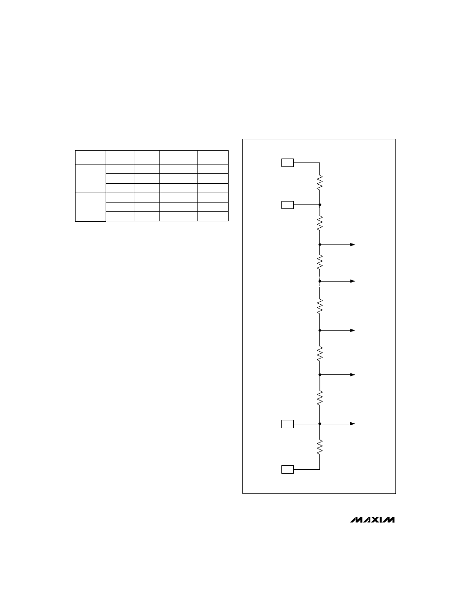
Reference
The ADC’s reference resistor is a Kelvin-sensed, resis-
tor string that sets the ADC’s LSB size and dynamic
operating range. Normally, the top and bottom of this
string are driven with an external buffer amplifier. It will
need to supply approximately 19mA due to the 100
Ω
minimum resistor string impedance. A ±0.95V refer-
ence voltage is normally applied to inputs VA
RT
, VB
RT
,
VA
RB
, and VB
RB
. The reference inputs VA
RTS
, VA
RBS
,
VB
RTS
, and VB
RBS
allow Kelvin sensing of the applied
voltages to increase precision.
An RC network at the ADC’s reference terminals is
needed for best performance. This network consists of
a 33
Ω
resistor connected in series with the buffer out-
put that drives the reference. A 0.47µF capacitor must
be connected near the resistor at the buffer’s output
(see
Typical Operating Circuit). This resistor and
capacitor combination should be located within 0.5
inches of the MAX101A package. Any noise on these
pins will directly affect the code uncertainty and
degrade the ADC’s effective-bits performance.
R
R
R
PARASITIC
RESISTANCE
TO
COMPARATORS
POSITIVE
REFERENCE
NEGATIVE
REFERENCE
R
R
VA
RBS
VA
RB
VA
RT
VA
RTS
PARASITIC
RESISTANCE
Figure 5. Reference Ladder
Table 2. Input Voltage Range
* An offset V
IO
, as specified in the DC electrical parameters, will
be present at the input. Compensate for this offset by adjusting
the reference voltage. Offsets may be different between side A
and side B.
INPUT
AIN+
(mV)
AIN-
(mV)
OUTPUT
CODE
MSB to
LSB
+125
-125
1 1 1 1 1 1 1 1
full scale
Differential
0
0
1 0 0 0 0 0 0 0
mid scale
-125
+125
0 0 0 0 0 0 0 0 zero scale
+250
0
1 1 1 1 1 1 1 1
full scale
0
0
1 0 0 0 0 0 0 0
mid scale
-250
0
0 0 0 0 0 0 0 0 zero scale
Single
Ended