Rainbow Electronics MAX1847 User Manual
Page 12
MAX1846/MAX1847
High-Efficiency, Current-Mode,
Inverting PWM Controller
12
______________________________________________________________________________________
Calculate the Duty Cycle
The duty cycle is the ratio of the on-time of the MOSFET
switch to the oscillator period. This is determined by the
ratio of the input voltage to the output voltage. Since
the input voltage typically has a range of operation, a
minimum (D
MIN
) and maximum (D
MAX
) duty cycle is
calculated by:
where V
D
is the forward drop across the output diode,
V
SW
is the drop across the external FET when on, and
V
LIM
is the current-limit threshold. To begin with,
assume V
D
= 0.5V for a Schottky diode, V
SW
= 100mV,
and V
LIM
= 100mV. Remember that V
OUT
is negative
when using this formula.
Setting the Output Voltage
The output voltage is set using two external resistors to
form a resistive-divider to FB between the output and
REF (refer to R1 and R2 in Figure 1). V
REF
is nominally
1.25V and the regulation voltage for FB is nominally 0.
The load presented to the reference by the feedback
resistors must be less than 500µA. This is to guarantee
that V
REF
is in regulation (see Electrical Characteristics
Table). Conversely, the current through the feedback
resistors must be large enough so that the leakage cur-
rent of the FB input (50nA) is insignificant. Therefore,
select R2 so that I
R2
is between 50µA and 250µA.
I
R2
= V
REF
/ R2
where V
REF
= 1.25V. A typical value for R2 is 10k
Ω.
Once R2 is selected, calculate R1 with the following
equation:
R1 = R2 x (-V
OUT
/ V
REF
)
Setting the Operating Frequency
The MAX1846/MAX1847 are capable of operating at
switching frequencies from 100kHz to 500kHz. Choice
of operating frequency depends on a number of fac-
tors:
1)
Noise considerations may dictate setting (or syn-
chronizing) f
OSC
above or below a certain fre-
quency or band of frequencies, particularly in RF
applications.
D
V
V
V
V
V
V
V
MAX
OUT
D
IN MIN
SW
LIM
OUT
D
=
+
+
−
−
−
−
(
)
D
V
V
V
V
V
V
V
MIN
OUT
D
IN MAX
SW
LIM
OUT
D
=
+
+
−
−
−
−
(
)
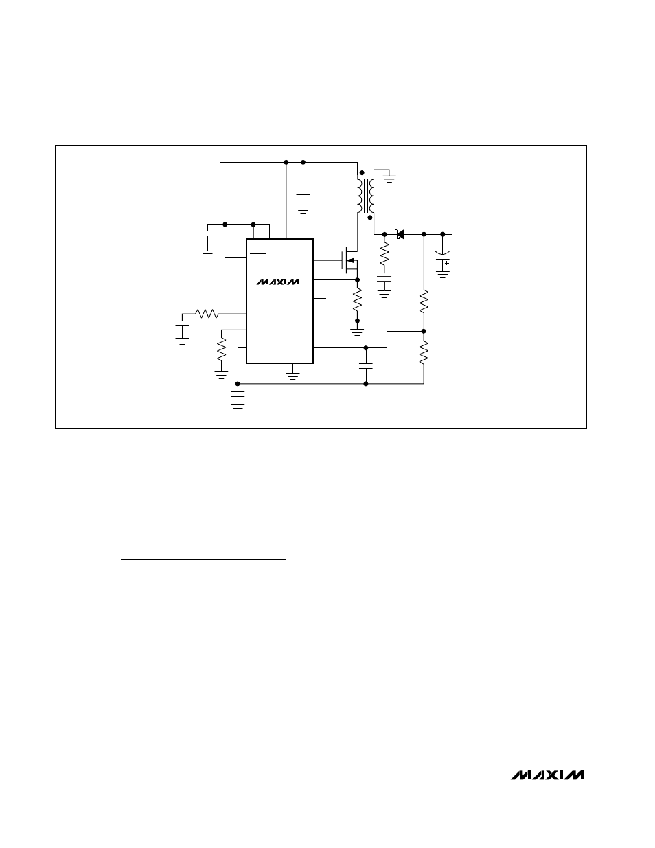
COMP
0.033
µF
270k
Ω
SYNC
150k
Ω
GND
FREQ
VL
V
IN
+12V
V
OUT
-48V AT 100mA
12
µF
100V
12
µF
25V
2
14
13
12
6
5
3
4
0.05
Ω
0.5W
1800pF
15
0.47
µF
0.1
µF
10, 11
EXT
PGND
REF
IN
CS
FB
N.C.
MAX1847
10.0k
Ω
1%
383k
Ω
1%
7, 9
POL
1
8
16
VP1-0190
12.2
µH
1:4
CMR1U-02
470
Ω
100pF
100V
SHDN
IRLL2705
Figure 1. Using an N-Channel MOSFET (MAX1847 only)