Applications information, Table 2. unipolar code table – Rainbow Electronics MAX5351 User Manual
Page 12

MAX535/MAX5351
Low-Power, 13-Bit Voltage-Output DACs
with Serial Interface
12
______________________________________________________________________________________
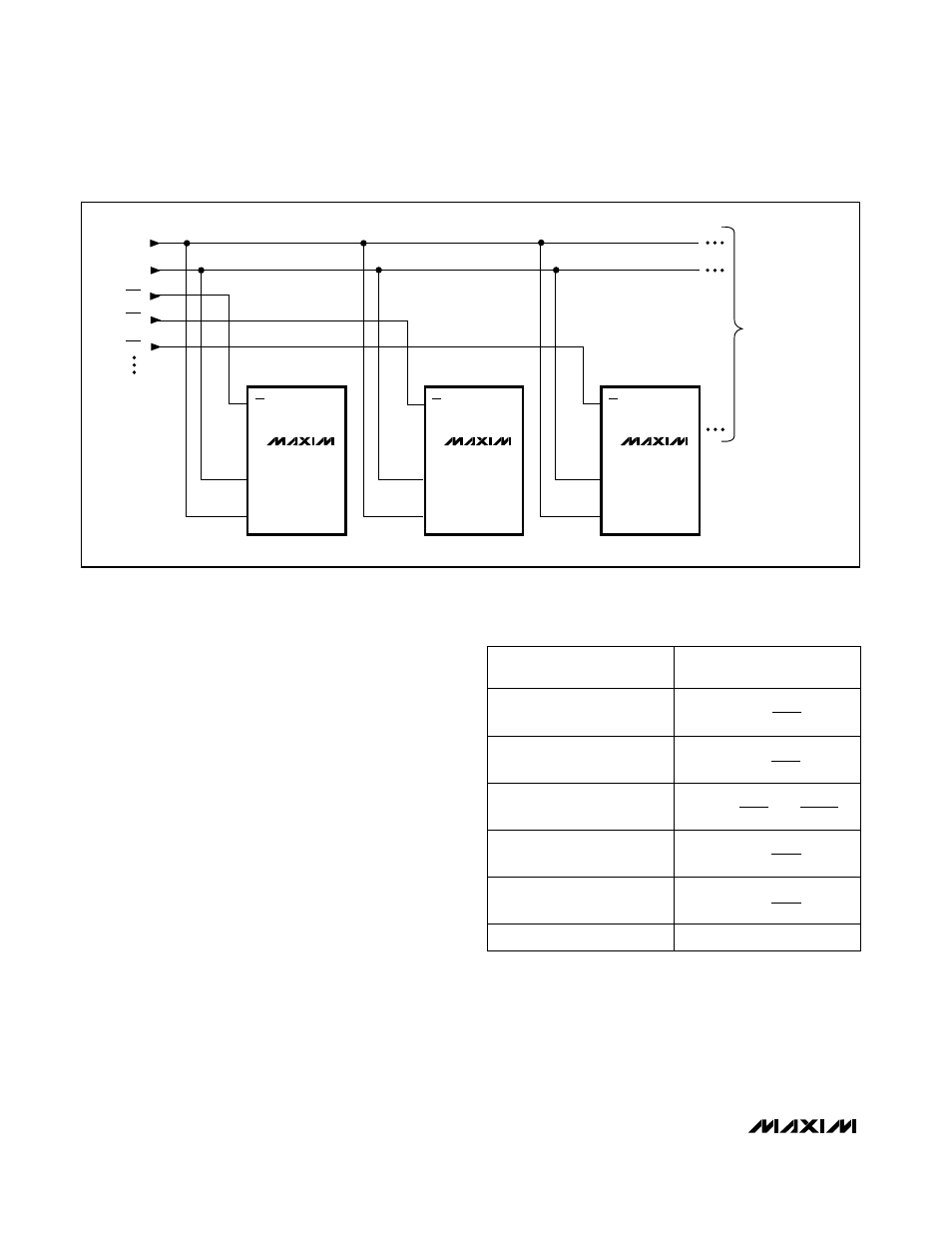
Figure 7 shows a method of connecting several
MAX535/MAX5351s. In this configuration, the clock and
the data bus are common to all devices and separate
chip-select lines are used for each IC.
__________Applications Information
Unipolar Output
For a unipolar output, the output voltage and the refer-
ence input have the same polarity. Figure 8 shows the
MAX535/MAX5351 unipolar output circuit, which is also
the typical operating circuit. Table 2 lists the unipolar
output codes.
For rail-to-rail output, see Figure 9. This circuit shows
the MAX535/MAX5351 with the output amplifier config-
ured with a closed-loop gain of +2 to provide 0V to 5V
full-scale range when a 2.5V reference is used. When
using the MAX5351 with a 1.25V reference, this circuit
provides a 0V to 2.5V full-scale range.
Bipolar Output
The MAX535/MAX5351 output can be configured for
bipolar operation using Figure 10’s circuit.
V
OUT
= V
REF
[(2NB / 8192) - 1]
where NB is the numeric value of the DAC’s binary input
code. Table 3 shows digital codes (offset binary) and
the corresponding output voltage for Figure 10’s circuit.
Using an AC Reference
In applications where the reference has AC-signal com-
ponents, the MAX535/MAX5351 have multiplying capa-
bility within the reference input range specifications.
Figure 11 shows a technique for applying a sine-wave
signal to the reference input where the AC signal is off-
set before being applied to REF. The reference voltage
must never be more negative than GND.
TO OTHER
SERIAL DEVICES
MAX535
MAX5351
DIN
SCLK
CS
MAX535
MAX5351
DIN
SCLK
CS
MAX535
MAX5351
DIN
SCLK
CS
DIN
SCLK
CS1
CS2
CS3
Figure 7. Multiple MAX535/MAX5351s Sharing Common DIN and SCLK Lines
Table 2. Unipolar Code Table
ANALOG OUTPUT
1 1 1 1 1
1 1 1 1
1 1 1 1
1 0 0 0 0
0 0 0 0
0 0 0 1
DAC CONTENTS
MSB
LSB
1 0 0 0 0
0 0 0 0
0 0 0 0
0 1 1 1 1
1 1 1 1
1 1 1 1
0 0 0 0 0
0 0 0 0
0 0 0 0
0V
0 0 0 0 0
0 0 0 0
0 0 0 1
+V
8191
8192
REF
+V
4097
8192
REF
+V
4096
8192
REF
=
+
V
REF
2
+V
4095
8192
REF
+V
1
8192
REF
