Rainbow Electronics MAX480 User Manual
Page 2
MAX480
High-Precision, Low-Voltage,
Micropower Op Amp
2
_______________________________________________________________________________________
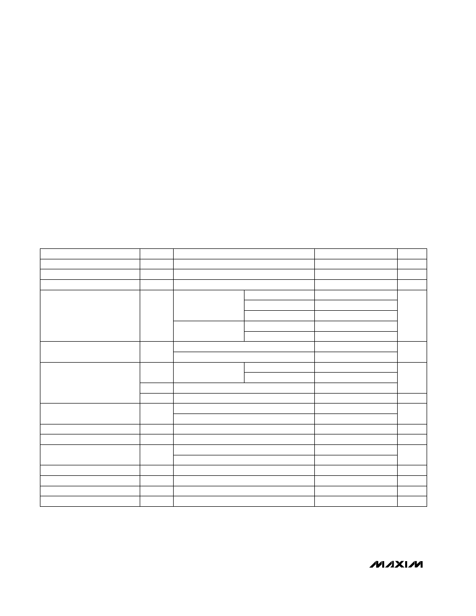
ABSOLUTE MAXIMUM RATINGS
ELECTRICAL CHARACTERISTICS
(V
S
= ±1.5V to ±15V, T
A
= +25°C, unless otherwise noted.)
Stresses beyond those listed under “Absolute Maximum Ratings” may cause permanent damage to the device. These are stress ratings only, and functional
operation of the device at these or any other conditions beyond those indicated in the operational sections of the specifications is not implied. Exposure to
absolute maximum rating conditions for extended periods may affect device reliability.
Supply Voltage (V+ to V-) ....................................................±18V
Differential Input Voltage ........................(V- - 20V) to (V+ + 20V)
Common-Mode Input Voltage ................(V- - 20V) to (V+ + 20V)
Output Short-Circuit Duration ........................................Indefinite
Continuous Power Dissipation
Plastic DIP (derate 9.09mW/°C above +70°C) .............727mW
SO (derate 5.88mW/°C above +70°C) ..............................471mW
CERDIP (derate 8.0mW/°C above +70°C) ....................640mW
Operating Temperature Ranges
MAX480C_A.........................................................0°C to +70°C
MAX480E_A ......................................................-40°C to +85°C
MAX480MJA ...................................................-55°C to +125°C
Junction Temperature (T
J
).................................-65°C to +150°C
Storage Temperature Range .............................-65°C to +150°C
Lead Temperature (soldering, 10sec) .............................+300°C
f
O
= 0.1Hz to 10Hz, V
S
= ±15V
A
V
= +1V/V, no oscillations (Note 2)
V
CM
= 0
V
S
= ±15V
V
CM
= 0
V+ = 5V, V- = 0, R
L
= 10k
Ω
V+ = 5V, V- = 0, R
L
= 2k
Ω
V+ = 5V, V- = 0
V
S
= ±15V
V
S
= ±15V,
V
O
= ±10V
CONDITIONS
µVp-p
3
e
np-p
Input Noise Voltage
pF
250
650
Capacitive Load Stability
µA
9
15
I
SY
Supply Current
V/ms
5
12
SR
Slew Rate
µV/V
1.0
12
PSRR
Power-Supply Rejection Ratio
V
100
500
V
O
4.0
4.2
±14
±14.2
V
0/4
IVR
Input Voltage
nA
1
3
I
B
Input Bias Current
nA
0.2
1
I
OS
µV
25
140
V
OS
Input Offset Voltage
Input Offset Current
V/mV
500
1200
UNITS
MIN
TYP
MAX
SYMBOL
PARAMETER
V
S
= ±15V
V
S
= ±15V
G
Ω
20
R
INCM
Common-Mode Input Resistance
M
Ω
30
R
IN
Differential-Mode Input Resistance
V
OL
V
OH
Output Voltage Swing
V+ = 5V, V- = 0, 0 < V
CM
< 4V
dB
85
110
CMRR
Common-Mode Rejection Ratio
V
S
= ±1.5V
µV
R
L
= 100k
Ω
R
L
= 2k
Ω
R
L
= 10k
Ω
75
250
200
600
R
L
= 100k
Ω
V+ = 5V, V- = 0,
1V < V
O
< 4V
R
L
= 10k
Ω
A
VO
Large-Signal Voltage Gain
50
180
100
400
V
S
= ±15kV (Note 1)
-15/13.5
R
L
= 10k
Ω
R
L
= 2k
Ω
±11
±12
V
S
= ±15V, -15V < V
CM
< 13.5V
90
130
V
S
= ±15V
14
20