Functional description – Rainbow Electronics LM80 User Manual
Page 13

Functional Description
(Continued)
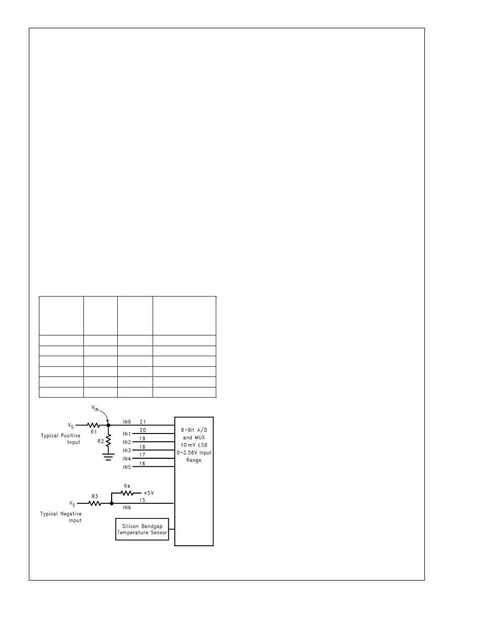
A typical application, such as is shown in
Figure 6, might
select the input voltage divider to provide 1.9V at the analog
inputs of the LM80. This is sufficiently high for good resolu-
tion of the voltage, yet leaves headroom for upward excur-
sions from the supply of about 25%. To simplify the process
of resistor selection, set the value of R2 first. Select a value
for R2 or R4 between 10 k
Ω
and 100 k
Ω
This is low enough
to avoid errors due to input leakage currents yet high enough
to both protect the inputs under overdrive conditions as well
as minimize loading of the source. Then select R1 or R3 to
provide a 1.9V input as show in
Figure 6.
For positive input voltages the equation for calculating R1 is
as follows:
R1 = [ (V
S
− V
IN
) / V
IN
] R2
For negative input voltages the equation for Calculating R3
is as follows:
R3 = [ (V
S
− V
IN
) / (V
IN
− 5V)] R4
The analog inputs have internal diodes that clamp inputs
exceeding the power supply and ground. Exceeding any
analog input has no detrimental effect on other channels.
The input diodes will also clamp voltages appearing at the
inputs of an un-powered LM80. External resistors should be
included to limit input currents to the values given in the
ABSOLUTE MAXIMUM RATINGS for Input Current At Any
Pin. Inputs with the attenuator networks will usually meet
these requirements. If it is possible for inputs without attenu-
ators to be turned on while LM80 is powered off, additional
resistors of about 10 k
Ω
should be added in series with the
inputs to limit the input current.
Voltage
Measure-
ments
(V
S
)
R1 or
R3
R2 or
R4
Voltage
at
Analog Inputs
( ADC code 190)
+2.5V
23.7 k
Ω
75 k
Ω
+1.9V
+3.3V
22.1 k
Ω
30 k
Ω
+1.9V
+5.0V
24 k
Ω
14.7 k
Ω
+1.9V
+12V
160 k
Ω
30.1 k
Ω
+1.9V
−12V
160 k
Ω
35.7 k
Ω
+1.9V
−5V
36 k
Ω
16.2 k
Ω
+1.9V
5.0 LAYOUT AND GROUNDING
Analog inputs will provide best accuracy when referred to the
AGND pin or a supply with low noise. A separate,
low-impedance ground plane for analog ground, which pro-
vides a ground point for the voltage dividers and analog
components, will provide best performance but is not man-
datory. Analog components such as voltage dividers should
be located physically as close as possible to the LM80.
The power supply bypass, the parallel combination of 10 µF
(electrolytic or tantalum) and 0.1 µF (ceramic) bypass ca-
pacitors connected between pin 9 and ground, should also
be located as close as possible to the LM80.
DS100040-11
FIGURE 6. Input Examples. Resistor values shown in
table provide approximately 1.9V at the analog inputs.
LM80
www.national.com
13
