Ac electrical characteristics—2.7v operation – Rainbow Electronics LMX339 User Manual
Page 2
LMX331/LMX393/LMX339
General-Purpose, Low-Voltage,
Single/Dual/Quad, Tiny-Pack Comparators
2
_______________________________________________________________________________________
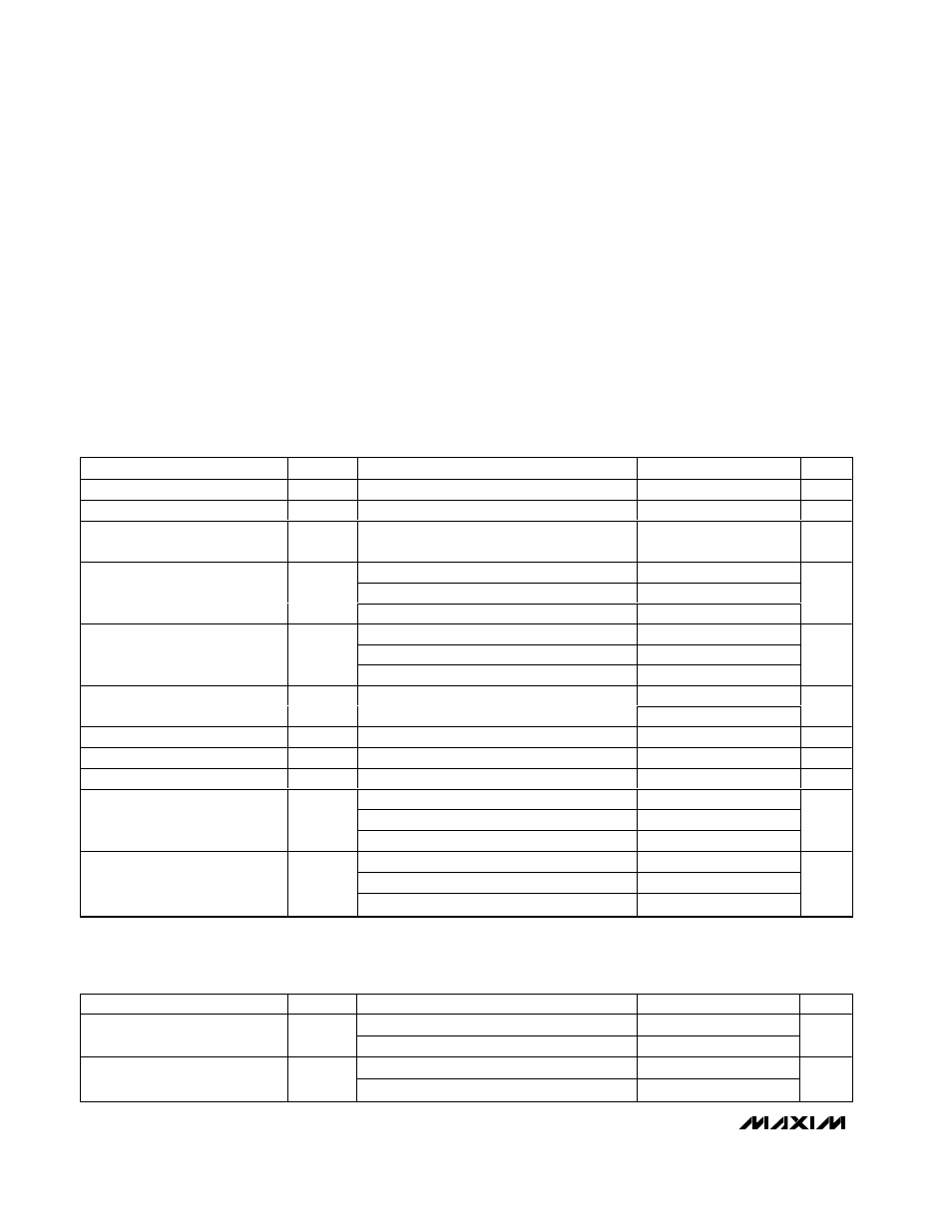
ABSOLUTE MAXIMUM RATINGS
DC ELECTRICAL CHARACTERISTICS—2.7V OPERATION
(V
DD
= 2.7V, V
SS
= 0, V
CM
= 0, R
L
= 5.1k
Ω connected to V
DD
. Typical values are at T
A
= +25
°C.) (Note 1)
Stresses beyond those listed under “Absolute Maximum Ratings” may cause permanent damage to the device. These are stress ratings only, and functional
operation of the device at these or any other conditions beyond those indicated in the operational sections of the specifications is not implied. Exposure to
absolute maximum rating conditions for extended periods may affect device reliability.
Supply Voltage (VDD to VSS)...................................-0.3V to +6V
All Other Pins .................................. (V
SS
- 0.3V) to (V
DD
+ 0.3V)
Continuous Power Dissipation (TA = +70°C)
5-Pin SC70 (derate 3.1mW/°C above +70°C) ..............247mW
5-Pin SOT23 (derate 7.1mW/°C above +70°C)............571mW
8-Pin SOT23 (derate 8.9mW/°C above +70°C)............714mW
8-Pin µMAX (derate 10.3mW/°C above +70°C) ...........825mW
14-Pin TSSOP (derate 9.1mW/°C above +70°C) .........727mW
14-Pin SO (derate 8.3mW/°C above +70°C).............666.7mW
Operating Temperature Range .........................-40°C to +125°C
Junction Temperature ......................................................+150°C
Storage Temperature Range .............................-65°C to +150°C
Lead Temperature (soldering, 10s) .................................+300°C
PARAMETER
SYMBOL
CONDITIONS
MIN
TYP
MAX
UNITS
Input Offset Voltage
V
OS
0.2
7
mV
Input Voltage Hysteresis
V
HYST
LMX331H/LMX393H/LMX339H only
2
mV
Input Offset Voltage Average
Temperature Drift
TCV
OS
5
µV/°C
T
A
= +25°C
±0.05
±250
T
A
= -40°C to +85°C
±400
Input Bias Current
I
B
T
A
= -40°C to +125°C
±400
nA
T
A
= +25°C
±0.05
±50
T
A
= -40°C to +85°C
±150
Input Offset Current
I
OS
T
A
= -40°C to +125°C
±150
nA
-0.1
Input Voltage Range
V
CM
2.0
V
Voltage Gain
A
V
LMX331/LMX393/LMX339 only
50
V/mV
Output Saturation Voltage
V
SAT
I
SINK
≤ 1mA
50
mV
Output Sink Current
I
O
V
O
≤ 1.5V
5
37
mA
LMX331/LMX331H
50
100
LMX393/LMX393H (both comparators)
70
140
Supply Current (Note 2)
I
S
LMX339/LMX339H (all four comparators)
140
200
µA
T
A
= +25°C
0.003
T
A
= -40°C to +85°C
1
Output Leakage Current
T
A
= -40°C to +125°C
2
µA
AC ELECTRICAL CHARACTERISTICS—2.7V OPERATION
(V
DD
= 2.7V, V
SS
= 0, V
CM
= 0, R
L
= 5.1k
Ω connected to V
DD
. Typical values are at T
A
= +25
°C.) (Note 1)
PARAMETER
SYMBOL
CONDITIONS
MIN
TYP
MAX
UNITS
Input overdrive = 10mV (Note 3)
500
Propagation Delay
Output High to Low
t
PHL
Input overdrive = 100mV (Note 3)
100
ns
Input overdrive = 10mV (Note 3)
500
Propagation Delay
Output Low to High
t
PLH
Input overdrive = 100mV (Note 3)
100
ns