Chip information – Rainbow Electronics MAX881R User Manual
Page 7
MAX881R
Low-Noise Bias Supply in µMAX
with Power-OK for GaAsFET PA
_______________________________________________________________________________________
7
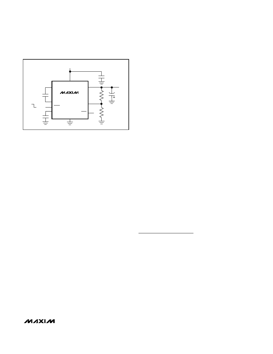
Capacitors
Use capacitors with a low effective series resistance
(ESR) to maintain a low dropout voltage (V
IN
- |V
OUT
|).
The overall dropout voltage is a function of the output
resistance of the charge pump and the voltage drop
across the linear regulator (N-channel pass transistor).
At the 100kHz charge-pump switching frequency, out-
put resistance is a function of the value of C1 and the
ESR of C1 and C2. Therefore, increasing C1 and mini-
mizing the ESR of the charge-pump capacitors mini-
mizes dropout voltage.
The output resistance of the entire circuit (in dropout) is
approximately:
R
OUT
= R
O
+ 4 x ESR
C1
+ ESR
C2
+ 1 / (f
S
x C1)
+ R
(linear regulator)
Where R
(linear regulator)
(the output impedance of the
linear regulator) is approximately 2
Ω
and R
O
(the resis-
tance of the internal switches) is typically 10
Ω
. When
regulating, the output resistance of the circuit is simply
the linear-regulator load regulation (2mV/mA).
C1, C2, and C3 should be 0.22µF capacitors with less
than 0.4
Ω
ESR. C4 should be a 4.7µF capacitor with
less than 0.1
Ω
ESR. Larger capacitor values can be
used (C1 = C2 = C3 = 1µF, C4 = 10µF) to reduce out-
put noise and ripple (1mVp-p), at the expense of cost
and board space. All capacitors should be either
ceramic or surface-mount chip tantalum (Figures 3a
and 3b).
Layout and Grounding
Good layout is important for good noise performance.
To optimize the layout:
1) Mount all components as close together as possible.
2) Keep traces short to minimize parasitic inductance
and capacitance, especially connections to FB.
3) Use a ground plane.
Noise and Ripple Measurement
Accurately measuring the output noise and ripple is a
challenge. Slight momentary differences in ground
potential between the circuit and the oscilloscope
(which result from the charge pump’s switching action)
cause ground currents in the probes’ wires, inducing
sharp voltage spikes. For best results, measure directly
across the output capacitor (C4). Do not use the
ground lead of the probe; instead, remove the probe’s
tip cover and touch the ground ring on the probe
directly to C4’s ground terminal. This direct connection
gives the most accurate noise and ripple measurement.
NEGOUT
SHDN
C1-
C1+
POK
FB
C3
0.22
µ
F
C2
0.22
µ
F
C1
0.22
µ
F
C4
4.7
µ
F
V
IN
OUT
R2
R1
IN
GND
MAX881R
ON
OFF
Figure 4. Adjustable Output Configuration
TRANSISTOR COUNT: 413
Chip Information