Detailed description, Applications information, Power-ok signal – Rainbow Electronics MAX881R User Manual
Page 6: Shutdown mode, Setting the output voltage
MAX881R
Low-Noise Bias Supply in µMAX
with Power-OK for GaAsFET PA
6
_______________________________________________________________________________________
________________Detailed Description
The MAX881R, a low-noise, inverting, regulated charge-
pump power supply, is designed for biasing GaAsFET
devices such as power-amplifier modules in cellular
handsets.
The applied input voltage (V
IN
) is inverted to a negative
voltage at NEGOUT by a capacitive charge pump. This
voltage is regulated by an internal linear regulator at
OUT (Figure 1). With FB connected to GND, V
OUT
is
regulated at -2V. Alternatively, use a voltage-divider at
FB to adjust the output voltage between -0.5V and -(V
IN
- 0.6V) (see the section
Setting the Output Voltage
).
The internal linear regulator reduces the ripple noise
induced by the charge-pump inverter to 1mVp-p at
OUT (circuit of Figure 3b). In addition, the excellent AC
rejection of the linear regulator attenuates noise from
the incoming supply.
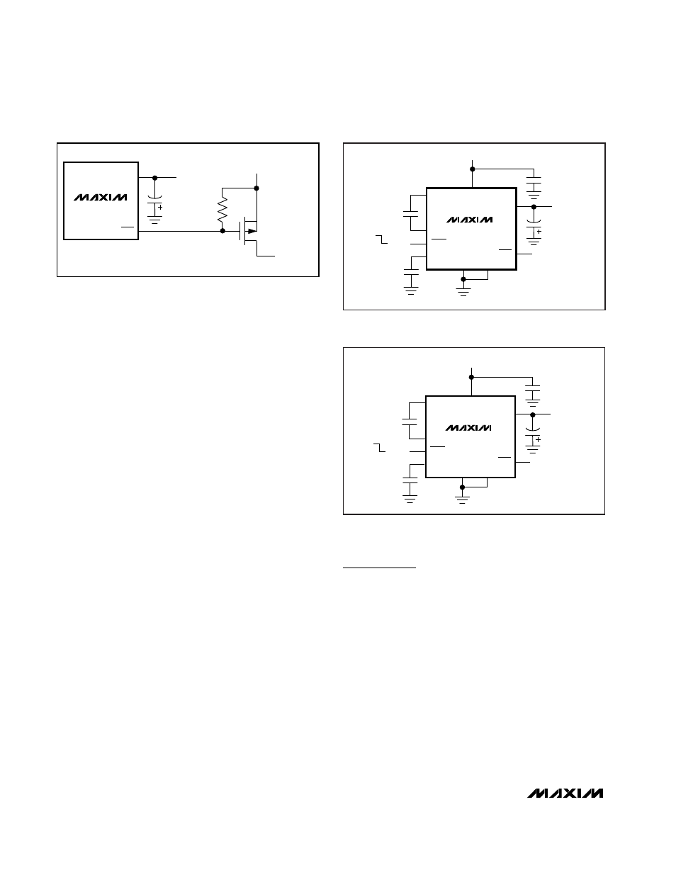
Power-OK Signal
The MAX881R has an active-low, open-drain, power-OK
(POK) output. This output goes low when OUT reaches
92.5% of the regulated output voltage. POK can be
used to drive the gate of a P-MOSFET that switches
power to the GaAsFET power amplifier (Figure 2), there-
by ensuring that the power amplifier is not powered
before the required negative bias voltage is present.
Use a 50k
Ω
or larger pull-up resistor to signal a logic
high when POK goes high impedance.
Shutdown Mode
The MAX881R features a shutdown mode that reduces
supply current to less than 1µA over temperature. SHDN
is an active-low, logic-level input. Start-up time coming
out of shutdown mode is typically 0.5ms. OUT and
NEGOUT are switched to GND in shutdown mode.
Applications Information
Setting the Output Voltage
Select either a fixed or adjustable output for the
MAX881R. Connect FB to GND for a fixed -2V output
(Figure 3). Select an alternative output voltage by con-
necting FB to the midpoint of a resistor-divider from
OUT to GND (Figure 4). When operating under full load
(4mA), the voltage at IN should be at least 0.6V higher
than the absolute voltage required at OUT. Note that
the minimum input voltage required for operation is
2.5V, regardless of the desired output voltage.
Choose R1 to be between 100k
Ω
and 400k
Ω
and cal-
culate R2. For greater accuracy, use resistors with 1%
or better tolerance.
R2 = R1 (2 x
|
V
OUT
|
- 1)
POK
100k
C4
V
CC
FOR
POWER AMPLIFIER
TO PA
GATE BIAS
TO
POWER
AMPLIFIER
OUT
MAX881R
P
Figure 2. Using the
POK Function
NEGOUT
SHDN
C1-
C1+
POK
V
OUT
= -2V
C3
0.22
µ
F
C2
0.22
µ
F
C1
0.22
µ
F
C4
4.7
µ
F
ON
V
IN
OFF
OUT
IN
GND
FB
MAX881R
Figure 3a. Standard Application Circuit for Minimum Capacitor
Values
NEGOUT
SHDN
C1-
C1+
POK
V
OUT
= -2V
C3
1
µ
F
C2
1
µ
F
C1
1
µ
F
C4
10
µ
F
V
IN
OUT
IN
GND
FB
MAX881R
ON
OFF
Figure 3b. Standard Application Circuit for Minimum Output
Noise