Rainbow Electronics MAX881R User Manual
Page 2
MAX881R
Low-Noise Bias Supply in µMAX
with Power-OK for GaAsFET PA
2
_______________________________________________________________________________________
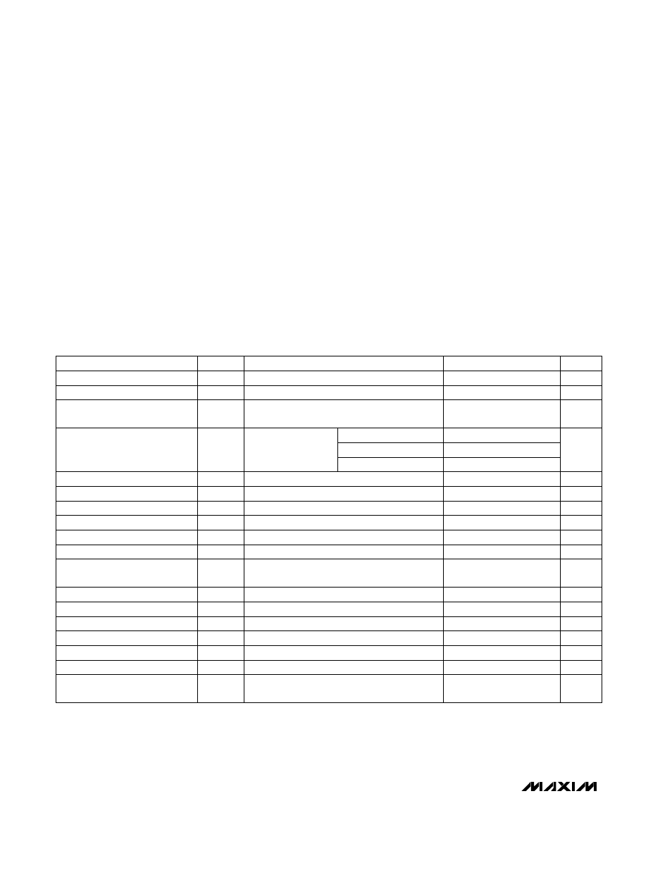
ABSOLUTE MAXIMUM RATINGS
ELECTRICAL CHARACTERISTICS
(Circuit of Figure 3, V
IN
= +3.6V, FB = GND, R
L
=
∞
, SHDN = IN,
T
A
= -40°C to +85°C
, unless otherwise noted. Typical values are at
T
A
= +25°C.) (Note 2)
Stresses beyond those listed under “Absolute Maximum Ratings” may cause permanent damage to the device. These are stress ratings only, and functional
operation of the device at these or any other conditions beyond those indicated in the operational sections of the specifications is not implied. Exposure to
absolute maximum rating conditions for extended periods may affect device reliability.
IN to GND .................................................................-0.3V to +6V
SHDN to GND...........................................................-0.3V to +6V
POK to GND ...........................................................-0.3V to +12V
C1+ to GND .................................................-0.3V to (V
IN
+ 0.3V)
C1-, NEGOUT, OUT, FB to GND ....................-6V to (V
IN
+ 0.3V)
Continuous Power Dissipation (T
A
= +70°C)
10-Pin µMAX (derate 5.6mW/°C above +70°C) ...........444mW
Operating Temperature Range ...........................-40°C to +85°C
Junction Temperature ......................................................+150°C
Storage Temperature Range .............................-65°C to +165°C
Lead Temperature (soldering, 10sec) .............................+300°C
V
IN
= 3V, R
L
= 500
Ω
, V
SHDN
= 0 to V
IN
,
POK goes low
V
IN
≥
2.5V, I
OUT
= 0 to 4mA
Connected to IN or GND
V
IN
= 2.5V
V
IN
≥
2.7V, I
OUT
= 0 to 4mA
V
IN
= 5.5V
V
POK
= 11V
I
OUT
= 4mA, circuit of Figure 3b
V
IN
≥
2.7V, I
OUT
= 0 to 4mA
V
IN
≥
2.5V, sinking 1mA
SHDN = GND
V
FB
= -0.5V
FB = OUT
CONDITIONS
ms
1
t
START
Start-Up Time
pF
10
C
IN
SHDN Input Capacitance
µA
±1
I
SHDN
SHDN Input Current
V
0.35
V
IL
SHDN Input Low Voltage
V
2.2
V
IH
SHDN Input High Voltage
µA
1
POK Off Leakage Current
mV
100
POK Output Level
% of
V
OUT
90
92.5
95
POK Threshold
kHz
80
100
120
f
OSC
Oscillator Frequency
V
-(V
IN
- 0.6)
-0.5
V
OUT
Adjustable Output Voltage
Range
V
-2.1
-2.0
-1.9
V
OUT
V
2.5
5.5
V
IN
Supply Voltage Range
Preset Output Voltage
mVp-p
1
Output Ripple
mV/mA
2
6
Output Load Regulation
µA
0.05
1
I
SHUT
Shutdown Supply Current
V
-0.515
-0.5
-0.485
V
FB
FB Voltage
nA
-10
-100
FB Input Current
µA
500
950
I
Q
Supply Current
UNITS
MIN
TYP
MAX
SYMBOL
PARAMETER
Note 1:
The output may be shorted to NEGOUT or GND if the package power dissipation is not exceeded. Typical short-circuit
current is 35mA.
-0.525
-0.475
-0.535
-0.465
V
IN
≥
2.5V,
I
OUT
= 0 to 4mA
T
A
= +25°C
T
A
= 0°C to +85°C
T
A
= -40°C to +85°C
Note 2:
Specifications to -40°C are guaranteed by design, not production tested.