Chip information, Table 1. partial listing of capacitor vendors, Layout considerations – Rainbow Electronics MAX1673 User Manual
Page 8

MAX1673
Regulated, 125mA-Output,
Charge-Pump DC-DC Inverter
Maxim cannot assume responsibility for use of any circuitry other than circuitry entirely embodied in a Maxim product. No circuit patent licenses are
implied. Maxim reserves the right to change the circuitry and specifications without notice at any time.
8
_____________________Maxim Integrated Products, 120 San Gabriel Drive, Sunnyvale, CA 94086 408-737-7600
© 1998 Maxim Integrated Products
Printed USA
is a registered trademark of Maxim Integrated Products.
The expression for the ripple component predominantly
due to charge transfer is:
where C
FLY
and C
OUT
are their respective capacitance
values, ESR
COUT
is the equivalent series resistance of
C
OUT
, R
OUT
is the MAX1673 open-loop output imped-
ance (typically 3.5
Ω
, and f
OSC
is the MAX1673 switch-
ing frequency (typically 350kHz). If ESR
COUT
is very
small, as is likely when ceramic capacitors are used,
V
RIPPLE (TRANSFER)
dominates. If ESR is relatively
large, as with low-cost tantalum capacitors, then V
RIP-
PLE (ESR)
dominates.
When operating in LIN mode, use the following equa-
tion to approximate peak-to-peak output voltage ripple:
where C
OUT
is the output capacitor value, ESR
COUT
is
the output capacitor’s ESR, and f
OSC
is the MAX1673
oscillator frequency (typically 350kHz).
To ensure LIN mode stability over the entire tempera-
ture range, choose a low-ESR (no more than 100m
Ω
)
output capacitance using the following equation:
where C
OUT
is the output capacitor value, and f
MIN
is
the minimum oscillator frequency (250kHz). See Table
1 for a list of suggested capacitor suppliers.
Layout Considerations
The MAX1673’s high oscillator frequency requires good
layout technique, which ensures stability and helps
maintain the output voltage under heavy loads. Take
the following steps to ensure good layout:
• Mount all components as close together as possible.
• Place the feedback resistors R1 and R2 close to the
FB pin, and minimize the PC trace length at the FB
circuit node.
• Keep traces short to minimize parasitic inductance
and capacitance.
• Use a ground plane.
COUT = 75 x 10
- 6
R1
R1 + R2
OUT
I
V
=
I
2 f
C
2I
ESR
RIPPLE
OUT
OSC
OUT
OUT
COUT
+
V
f
R
(C
C
)
RIPPLE(ESR)
= 2
V
IN
– V
OUT
OSC
1
OUT
FLY
OUT
+
V
8
f
R
C
RIPPLE(ESR)
=
V
IN
– V
OUT
OSC
ESR
COUT
2
OUT FLY
PRODUCTION METHOD
MANUFACTURER
SERIES
PHONE
FAX
Surface-Mount Tantalum
AVX
TPS
(803) 946-0690
(803) 448-2170
Matsuo
267
(714) 969-2491
(714) 960-6492
Sprague
593D, 595D
(603) 224-1961
(603) 224-1430
Surface-Mount Ceramic
AVX
X7R
(803) 946-0590
(803) 626-3123
Matsuo
X7R
(714) 969-2491
(714) 960-6492
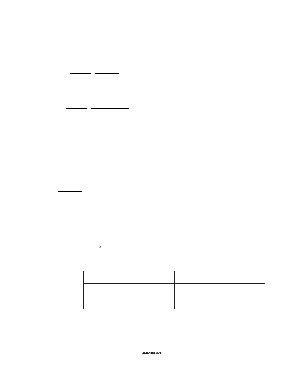
Table 1. Partial Listing of Capacitor Vendors
___________________Chip Information
TRANSISTOR COUNT: 386
SUBSTRATE CONNECTED TO: IN
