Applications information, Linear mode (constant-frequency mode), Skip mode – Rainbow Electronics MAX1673 User Manual
Page 7: Shutdown mode, Resistor selection (output voltage selection), Capacitor selection

Linear Mode (Constant-Frequency Mode)
In LIN mode (LIN/SKIP = IN), the charge pump runs con-
tinuously at 350kHz. The MAX1673 controls the charge
on C
FLY
by varying the gate drive on S1 (Figure 2).
When the output voltage falls, C
FLY
charges faster due
to increased gate drive. Since the device switches con-
tinuously, the regulation scheme minimizes output ripple,
the output noise contains well-defined frequency compo-
nents, and the circuit requires much smaller external
capacitors than in Skip mode for a given output ripple.*
However, LIN mode is less efficient than Skip mode due
to higher operating current (8mA typical).
Skip Mode
In Skip mode (LIN/SKIP = GND), the device switches
only as needed to maintain regulation on FB. Switching
cycles are skipped until the voltage on FB rises above
GND. Skip mode has higher output noise than LIN
mode, but minimizes operating current.
Shutdown Mode
When SHDN (a CMOS-compatible input) is driven low,
the MAX1673 enters low-power shutdown mode.
Charge-pump switching action halts and an internal 1
Ω
switch pulls V
OUT
to ground. Connect SHDN to IN or
drive high for normal operation.
*See Output Ripple vs. Load Current in
Typical Operating Characteristics.
Applications Information
Resistor Selection
(Output Voltage Selection)
The accuracy of V
OUT
depends on the accuracy of the
voltage biasing the voltage-divider network (R1, R2).
Use a separate reference voltage if V
IN
is an unregulat-
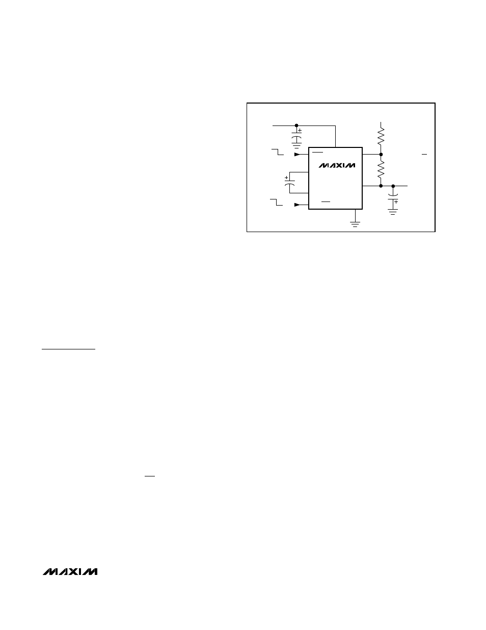
ed voltage or if greater accuracy is desired (Figure 4).
Adjust the output voltage from -1.5V to -V
IN
in LIN
mode or 0V to -V
IN
in Skip mode with external resistors
R1 and R2 as shown in Figures 1 and 4. In either regu-
lating mode (LIN or Skip), FB servos to 0V. Use the
following equations to select R1 and R2 for the desired
output voltage:
where V
REF
can be either V
IN
or some other positive
reference source.
Typically, choose a voltage-divider current of 50µA to
minimize the effect of FB input current:
R1 = V
REF
/ 50µA
R2 = -V
OUT
/ 50µA
Capacitor Selection
A C
FLY
value of 1µF or more is sufficient to supply the
specified load current. However, for minimum ripple in
Skip mode, this value may need to be increased.
Maxim recommends 2.2µF.
Surface-mount ceramic capacitors are preferred for
C
FLY
, due to their small size, low cost, and low equiva-
lent series resistance (ESR). To ensure proper opera-
tion over the entire temperature range, choose ceramic
capacitors with X7R (or equivalent) low-temperature-
coefficient (tempco) dielectrics. See Table 1 for a list of
suggested capacitor suppliers.
The output capacitor stores the charge transferred from
the flying capacitor and services the load between
oscillator cycles. A good general rule is to make the
output capacitance at least ten times greater than that
of the flying capacitor.
When in Skip mode, output ripple depends mostly on
two parameters: charge transfer between the capaci-
tance values of C
FLY
and C
OUT
, and the ESR of C
OUT
.
The ESR ripple contribution occurs as C
OUT
charges.
The charging current creates a negative voltage pulse
across the capacitor’s ESR that recedes as C
OUT
charges. At equilibrium, when the voltage on C
FLY
approaches that on C
OUT
, no charging current flows.
Secondly, the ripple contribution due to charge transfer
between capacitors creates a pulse as charge flows to
C
OUT
. Adding the two terms does not determine peak-
to-peak ripple because their peaks do not occur at the
same time. It is best to use only the dominant term. The
expression for the ripple component predominantly due
to C
OUT
ESR is:
V
= - V
R2
R1
OUT
REF
MAX1673
Regulated, 125mA-Output,
Charge-Pump DC-DC Inverter
_______________________________________________________________________________________
7
MAX1673
IN
INPUT
5.0V
OUTPUT
-3V
C
IN
10
µ
F
C
OUT
22
µ
F
C
FLY
2.2
µ
F
LIN/SKIP
FB
R1
100k
R2
60.4k
OUT
GND
CAP+
ON
OFF
4
2
3
SHDN
CAP-
LIN
SKIP
1
7
5
6
8
V
REF
5V
V
OUT
=
-V
REF
x
R2
R1
Figure 4. Separate V
REF
for Voltage Divider
