Recommended_operating_conditions, Absolute_maximum_ratings – Rainbow Electronics MAX31D80 User Manual
Page 2
Spread-Spectrum Clock Generators
MAX31C80/MAX31D80
2_ _ _______________________________________________________________________________________
Stresses beyond those listed under “Absolute Maximum Ratings” may cause permanent damage to the device. These are stress ratings only, and
functional operation of the device at these or any other conditions beyond those indicated in the operational sections of the specifications is not implied.
Exposure to absolute maximum rating conditions for extended periods may affect device reliability.
Voltage Range on V
CC
Relative to GND ..............-0.3V to +4.3V
Voltage Range on Any Other Pin
Relative to GND .................................... -0.3V to (V
CC
+ 0.3V)*
Continuous Power Dissipation (T
A
= +70°C)
10-Pin TDFN (derate 24.4mW/°C above +70°C) .....1951.2mW
Storage Temperature Range ............................ -55NC to +135NC
Lead Temperature (soldering, 10s) ................................+300NC
Soldering Temperature (reflow) ......................................+260NC
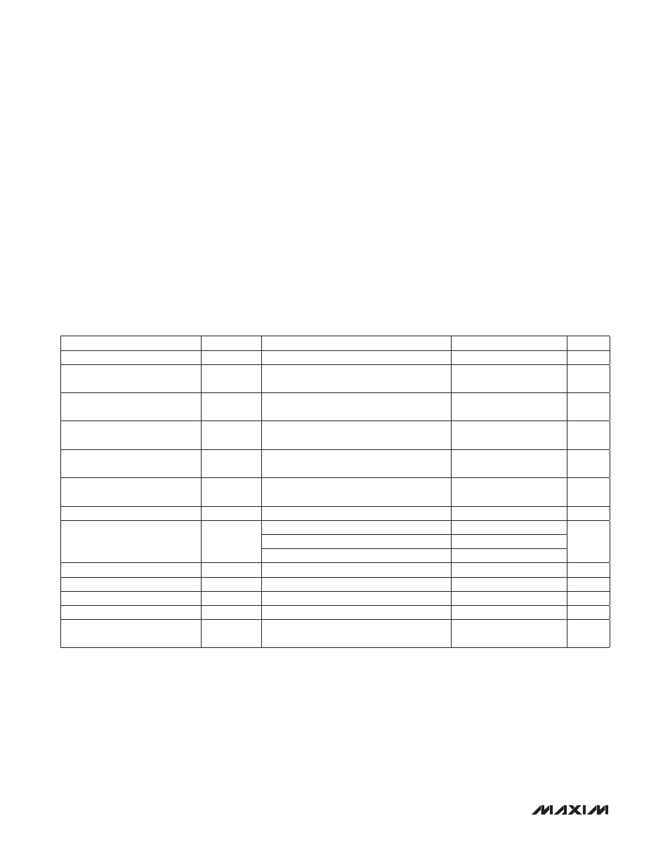
RECOMMENDED_OPERATING_CONDITIONS
(T
A
= -40NC to +125NC.)
ABSOLUTE_MAXIMUM_RATINGS
*Not to exceed +4.3V.
PARAMETER
SYMBOL
CONDITIONS
MIN
TYP
MAX
UNITS
Supply Voltage
V
CC
3.0
3.3
3.6
V
Input Logic 0
(SMSEL0 and SMSEL1)
V
IL
-0.3
0.25 x
V
CC
V
Input Logic 1
(SMSEL0 and SMSEL1)
V
IH
0.75 x
V
CC
V
CC
+
0.3
V
Input Logic Unconnected
(SMSEL0 and SMSEL1)
V
IF
Limits are in case user wants to force
voltage instead of unconnecting this pin
0.4 x
V
CC
0.55 x
V
CC
V
Input Logic 0 for X1
V
IL:X1
-0.3
0.3 x
V
CC
V
Input Logic 1 for X1
V
IH:X1
0.7 x
V
CC
V
CC
+
0.3
V
XOUT Load
C
L:XOUT
15
pF
CLKOUT Load
C
L:CLKOUT
2MHz P f
CLKOUT
< 67MHz
15
pF
67MHz P f
CLKOUT
< 101MHz
10
101MHz P f
CLKOUT
P 134MHz
7
Crystal Frequency
f
IN
8
34
MHz
Clock Input Frequency
f
IN
8
134
MHz
Crystal ESR
X
ESR
90
I
Clock Input Duty Cycle
f
INDC
40
60
%
Crystal Parallel Load
Capacitance
C
CL
18
pF