Ac electrical characteristics – Rainbow Electronics MAX2648 User Manual
Page 2
MAX2648
5GHz to 6GHz Low-Noise Amplifier
in 6-Pin UCSP
2
_______________________________________________________________________________________
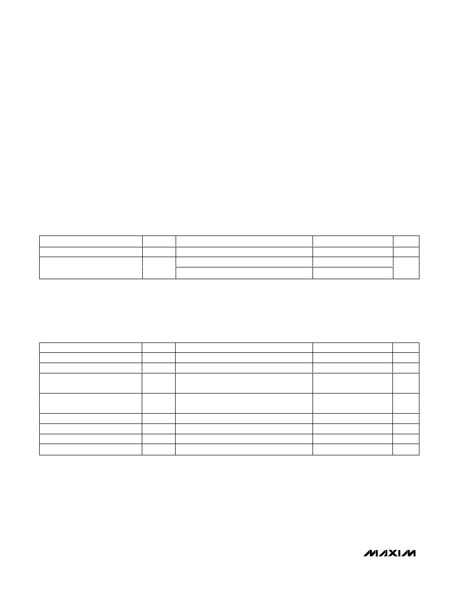
ABSOLUTE MAXIMUM RATINGS
DC ELECTRICAL CHARACTERISTICS
(V
CC
= +2.7V to +3.6V, no RF signals applied, RFIN and RFOUT terminated in 50
Ω through a DC-blocking capacitor, RFOUT con-
nected to V
CC
. Typical values for V
CC
= +3.0V, T
A
= +25°C, unless otherwise noted.)
Stresses beyond those listed under “Absolute Maximum Ratings” may cause permanent damage to the device. These are stress ratings only, and functional
operation of the device at these or any other conditions beyond those indicated in the operational sections of the specifications is not implied. Exposure to
absolute maximum rating conditions for extended periods may affect device reliability.
Note 1: Limits are guaranteed by design and characterization, and are not production tested.
V
CC
to GND ...........................................................-0.3V to +6.0V
RFOUT to GND......................................................-0.3V to +6.0V
RFIN.......................................................................-0.3V to +0.8V
RFIN Power (50
Ω source) ..............................................+15dBm
Continuous Power Dissipation
2
✕
3-Bump UCSP (derate 24mW/°C above +70°C) ......500mW
Operating Temperature .......................................-40°C to +85°C
Junction Temperature ......................................................+150°C
Storage Temperature.........................................-55°C to +150°C
PARAMETER
SYMBOL
CONDITIONS
MIN
TYP
MAX
UNITS
Supply Voltage Range
V
CC
2.7
3.6
V
T
A
= +25
°C
12.3
15
Supply Current
I
CC
T
A
= -40
°C to +85°C (Note 1)
18
mA
AC ELECTRICAL CHARACTERISTICS
(MAX2648 evaluation kit, V
CC
= +3.0V, f
IN
= 5250MHz, P
IN
= -30dBm, 50
Ω system, T
A
= +25°C. Typical values for V
CC
= +3.0V,
T
A
= +25°C, unless otherwise noted. All limits are guaranteed by design and characterization and are not production tested.)
PARAMETER
SYMBOL
CONDITIONS
MIN
TYP
MAX
UNITS
Frequency Range
f
IN
(Note 2)
5250
MHz
Power Gain
|S
21
|
(Note 3)
16
17.4
dB
Maximum Gain Variation over
Temperature
T
A
= -40°C to +85°C
0.2
1.0
dB
Input Third Order Intercept
IIP3
Two tones at 5250MHz and 5251MHz,
-30dBm per tone (Note 4)
-4.0
0
dBm
Noise Figure
NF
(Note 4)
1.8
2.3
dB
Input Return Loss
|S
11
|
-14
dB
Output Return Loss
|S
22
|
-14
dB
Reverse Isolation
|S
12
|
-31
dB
Note 2: The recommended operating range is 5100MHz to 5850MHz. Operation outside this frequency range is possible but has not
been characterized. The device is matched, characterized, and tested at 5250MHz. For optimum performance at a given
frequency, the input and output ports must be properly matched. See Applications Information section for more information
on matching.
Note 3: Specifications are corrected for board losses (0.4dB at input, 0.4dB at output)
Note 4: Specification is corrected for board losses (0.4dB at input)