5v, step-down, current-mode pwm dc-dc converters, Output filter capacitor selection, Other components – Rainbow Electronics MAX744A User Manual
Page 10
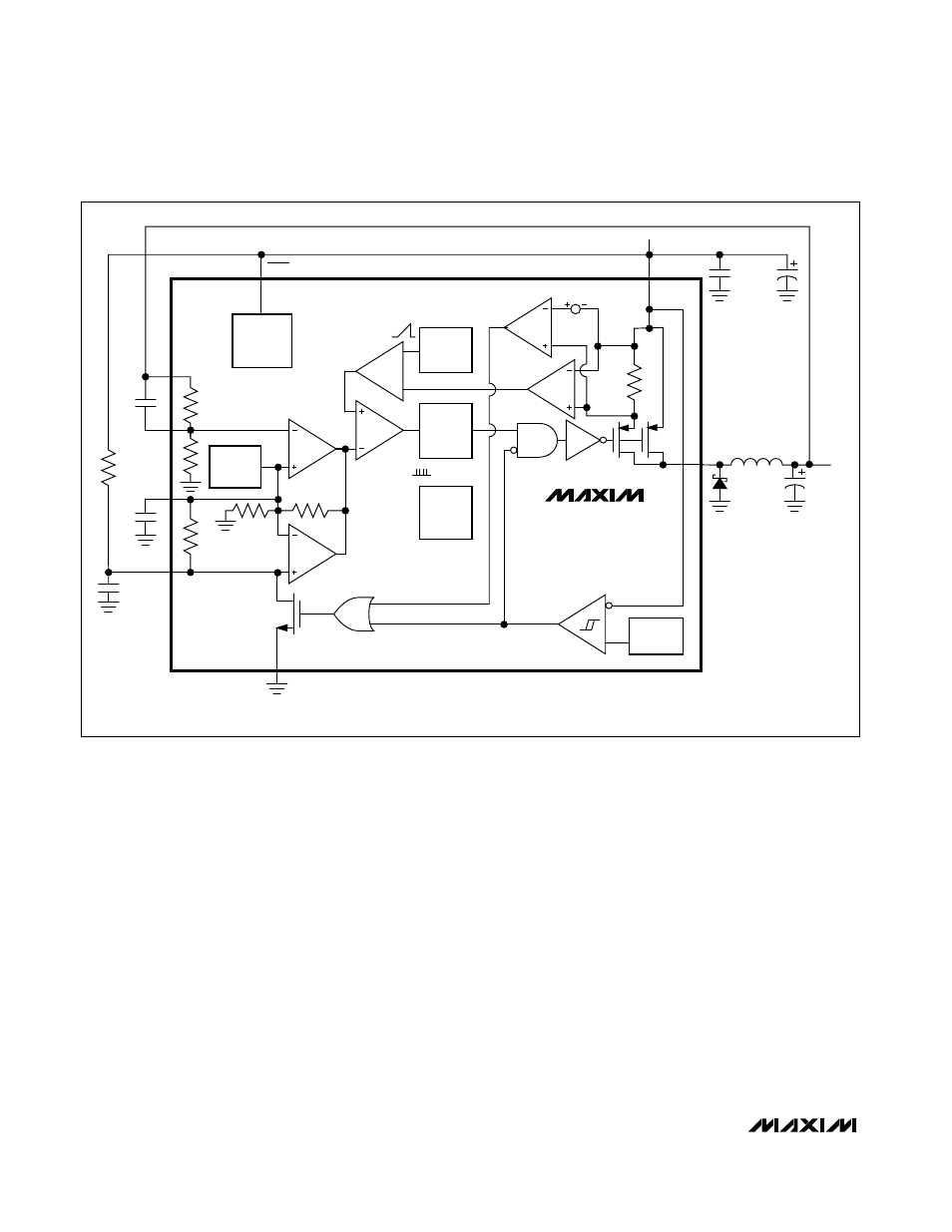
MAX730A/MAX738A/MAX744A
single 100µH (MAX7__AC) or 33µH (MAX7__AE/AM)
inductor. The inductor’s incremental saturation current
rating should be greater than 1A, and its DC resistance
should be less than 0.8
Ω
. Table 2 lists inductor types
and suppliers for various applications. The surface-
mount inductors have nearly equivalent efficiencies to
the larger through-hole inductors.
Output Filter Capacitor Selection
The primary criterion for selecting the output filter
capacitor is low equivalent series resistance (ESR).
The product of the inductor current variation and the
output capacitor’s ESR determines the amplitude of the
sawtooth ripple seen on the output voltage. Also, mini-
mize the output filter capacitor’s ESR to maintain AC
stability. The capacitor’s ESR should be less than
0.25
Ω
to keep the output ripple less than 50mVp-p over
the entire current range (using a 100µH inductor).
Capacitor ESR rises as the temperature falls, and
excessive ESR is the most likely cause of trouble at
temperatures below 0°C. Sanyo OS-CON series
through-hole and surface-mount tantalum capacitors
exhibit low ESR at temperatures below 0°C. Refer to
Table 2 for recommended capacitor values and sug-
gested capacitor suppliers.
Other Components
The catch diode should be a Schottky or high-speed
silicon rectifier with a peak current rating of at least
1.5A for full-load (750mA) operation. The 1N5817 is a
good choice. The 330pF outer-loop compensation
capacitor provides the widest input voltage range and
best transient characteristics. For low-current applica-
tions, the 510k
Ω
resistor may be omitted (see the
Maximum Output Current vs. Supply Voltage graph (R1
removed) in the
Typical Operating Characteristics
).
5V, Step-Down,
Current-Mode PWM DC-DC Converters
10
______________________________________________________________________________________
C1
0.1
µ
F
SS
REF
CC
OUT
C5
330pF
R1
510k
C6
0.01
µ
F
1M
±35%
GND
SS CLAMP
PWM
COMPARATOR
BIAS
GEN
SHDN
Σ
RAMP
GEN
SLOPE COMPENSATION
OVERCURRENT COMPARATOR
R
SENSE
CURRENT
SENSE AMP
V
IN
= +6.0V TO +16.0V
C2
1
µ
F
V+
C3
*
V
OUT
=
+5V
C4
*
D1
1N5817
LX
VUVLO
UNDERVOLTAGE
LOCKOUT
OSC
F/F
S
R
Q
1.23V
BANDGAP
ERROR AMP
*SEE TABLE 2 FOR COMPONENT VALUES AND SUPPLIERS
L1
MAX730A
MAX738A
MAX744A
Figure 1. Detailed Block Diagram with External Components