Analog considerations, Pipelined operation, Reference – Rainbow Electronics MAX117 User Manual
Page 9

that contain the conversion result (D0–D7).
INT also
goes low after the falling edge of
RD and is reset on the
rising edge of
RD or CS. The total conversion time is
therefore: t
WR
+ t
RD
+ t
ACC1
= 1800ns.
Pipelined Operation
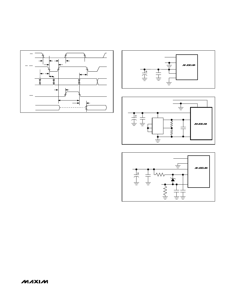
Besides the two standard write-read-mode options,
“pipelined” operation can be achieved by connecting
WR and RD together (Figure 6). With CS low, driving
WR and RD low initiates a conversion and concurrently
reads the result of the previous conversion.
_____________Analog Considerations
Reference
Figures 7a, 7b, and 7c show typical reference connec-
tions. The voltages at REF+ and REF- set the ADC’s
analog input range (Figure 10). The voltage at REF-
defines the input that produces an output code of all
zeros, and the voltage at REF+ defines the input that
produces an output code of all ones.
The internal resistance from REF+ to REF- can be as
low as 1k
Ω
, and current will flow through it even when
the MAX113/MAX117 are shut down. Figure 7d shows
how an N-channel MOSFET can be connected to REF-
to break this current path during power-down. The FET
should have an on-resistance of less than 2
Ω
with a 3V
gate drive. When REF- is switched, as in Figure 7d, a
new conversion can be initiated after waiting a time
equal to the power-up delay (t
UP
) plus the N-channel
FET’s turn-on time.
Although REF+ is frequently connected to V
DD
, the cir-
cuit of Figure 7d uses a low-current, low-dropout, 2.5V
voltage reference: the MAX872. Since the MAX872
cannot continuously furnish enough current for the ref-
erence resistance, this circuit is intended for applica-
tions where the MAX113/MAX117 are normally in stand-
by and are turned on in order to make measurements
at intervals greater than 100µs. C1 (the capacitor con-
nected to REF+) is slowly charged by the MAX872 dur-
ing the standby period, and furnishes the reference
current during the short measurement period.
The 4.7µF value of C1 ensures a voltage drop of less
than 1/2LSB when performing four to eight successive
conversions. Larger capacitors reduce the error still fur-
ther. Use ceramic or tantalum capacitors for C1.
MAX113/MAX117
+3V, 400ksps, 4/8-Channel,
8-Bit ADCs with 1µA Power-Down
_______________________________________________________________________________________
9
t
ACQ
t
INTL
RD, WR
INT
NEW DATA (N)
t
WR
t
ACQ
t
AH
t
CSH
t
IHWR
t
CSS
t
ID
OLD DATA (N - 1)
D0–D7
ADDRESS
VALID (N)
ADDRESS
VALID (N + 1)
A0–A2
CS
Figure 6. Pipelined Mode Timing (
WR = RD) (Mode = 1)
REF-
MAX113
MAX117
V
DD
IN_
REF+
V
IN+
V
IN-
GND
+3V
0.1
µ
F
4.7
µ
F
Figure 7a. Power Supply as Reference
+3V
0.1µF
4
REF-
MAX113
MAX117
REF+
IN_
8
1
3
7
0.1µF
4.7µF
2
6
GND
V
DD
+2.5V
34.8k
3.01k
LM10
V
IN+
V
IN-
REF-
MAX113
MAX117
REF+
0.1µF
0.1µF
* CURRENT PATH MUST STILL
EXIST FROM V
IN-
TO GND
R*
IN_
V
IN-
V
DD
V
IN+
GND
+3V
+2.5V
0.1µF
4.7µF
Figure 7b. External Reference, 2.5V Full Scale
Figure 7c. Input Not Referenced to GND
