Read mode (mode = 0), Write-read mode (mode = 1), Using internal delay – Rainbow Electronics MAX117 User Manual
Page 8: Fastest conversion: reading before delay
MAX113/MAX117
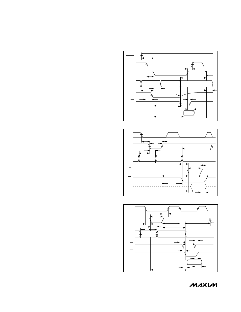
Read Mode (MODE = 0)
In read mode, conversions and data access are con-
trolled by the
RD input (Figure 3). The comparator
inputs track the analog input voltage for the duration of
t
ACQ
. A conversion is initiated by driving
CS and RD
low. With µPs that can be forced into a wait state, hold
RD low until output data appears. The µP starts the
conversion, waits, and then reads data with a single
read instruction.
In read mode,
WR/RDY is configured as a status output
(RDY), so it can drive the ready or wait input of a µP.
RDY is an open-collector output (no internal pull-up)
that goes low after the falling edge of
CS and goes high
at the end of the conversion. If not used, the
WR/RDY
pin can be left unconnected. The
INT output goes low
at the end of the conversion and returns high on the ris-
ing edge of
CS or RD.
Write-Read Mode (MODE = 1)
Figures 4 and 5 show the operating sequence for write-
read mode. The comparator inputs track the analog
input voltage for the duration of t
ACQ
. The conversion is
initiated by a falling edge of
WR. When WR returns
high, the result of the four-MSBs flash is latched into the
output buffers and the conversion of the four-LSBs flash
starts.
INT goes low, indicating conversion end, and the
lower four data bits are latched into the output buffers.
The data is then accessible after
RD goes low (see
Timing Characteristics
).
A minimum acquisition time (t
ACQ
) is required from
INT
going low to the start of another conversion (
WR going
low).
Options for reading data from the converter include
using internal delay, reading before delay, and pipelined
operation (discussed in the following sections).
Using Internal Delay
The µP waits for the
INT output to go low before reading
the data (Figure 4).
INT goes low after the rising edge of
WR, indicating that the conversion is complete and the
result is available in the output latch. With
CS low, data
outputs D0–D7 can be accessed by pulling
RD low. INT
is then reset by the rising edge of
CS or RD.
Fastest Conversion:
Reading Before Delay
An external method of controlling the conversion time is
shown in Figure 5. The internally generated delay
(t
INTL
) varies slightly with temperature and supply volt-
age, and can be overridden with
RD to achieve the
fastest conversion time.
RD is brought low after the ris-
ing edge of
WR, but before INT goes low. This com-
pletes the conversion and enables the output buffers
+3V, 400ksps, 4/8-Channel,
8-Bit ADCs with 1µA Power-Down
8
_______________________________________________________________________________________
t
CSS
t
RDY
t
ACQ
t
AH
WITH EXTERNAL
PULL-UP
t
CSH
t
ACQ
t
INTH
t
UP
t
DH
t
CRD
t
ACCO
D0–D7
RDY
RD
CS
PWRDN
INT
A0–A2
VALID DATA
(N)
ADDRESS VALID (N + 1)
ADDRESS VALID
(N)
t
AH
t
AH
t
ACQ
t
DH
t
READ2
t
RD
D0–D7
RD
WR
CS
INT
VALID DATA
(N)
t
INTL
t
ACC2
t
WR
t
CSS
t
CSH
t
ACQ
t
CSS
t
CSH
A0–A2
t
INTH
ADDRESS
VALID (N)
ADDRESS VALID (N + 1)
Figure 3. Read Mode Timing (Mode = 0)
Figure 4. Write-Read Mode Timing (t
RD
> t
INTL
) (Mode = 1)
t
CSS
t
ACQ
t
DH
t
READ1
t
RD
t
INTL
t
ACQ
t
AH
RD
WR
CS
INT
VALID DATA
(N)
t
CSS
t
CSH
t
INTH
t
WR
t
CSH
t
ACC1
t
CWR
t
RI
A0–A2
D0–D7
ADDRESS
VALID (N)
ADDRESS VALID (N + 1)
Figure 5. Write-Read Mode Timing (t
RD
< t
INTL
) (Mode = 1)