Pin description – Rainbow Electronics MAX2685 User Manual
Page 6
MAX2685
Low-Cost, 900MHz, Low-Noise Amplifier
and Downconverter Mixer
6
_______________________________________________________________________________________
Pin Description
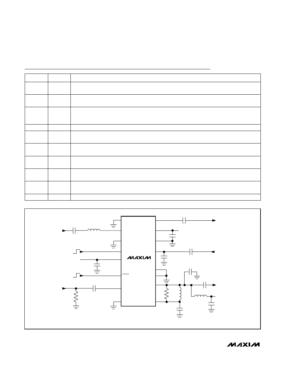
NAME
FUNCTION
1, 3, 8,
11, 12, 14
GND
Ground. Connect to ground plane with a low-inductance connection.
2
LNAIN
RF Input to LNA and LNA Bypass Switch. Requires an external matching network and a series
DC-blocking capacitor.
PIN
4
GAIN
Gain Control Logic-Level Input. Drive high to enable the LNA, open the LNA bypass switch, and
increase the receiver’s gain. Drive low to disable the LNA, close the LNA bypass switch, and reduce
the receiver’s gain.
5, 15
V
CC
Supply Voltage. Bypass V
CC
to GND at each pin with a 47pF capacitor as close to the pin as possible.
6
SHDN
Shutdown Control Logic-Level Input. Drive high or connect to V
CC
for normal operation. Drive low to
place the device in low-power shutdown mode.
7
LO
Local-Oscillator Input to Downconverter Mixer. Requires a series DC-blocking capacitor and an imped-
ance-setting resistor (typically 75
Ω to ground).
9
IFOUT-
Inverting Side to Downconverter Mixer’s Differential Open-Collector IF Output. Requires a pull-up induc-
tor to V
CC
for proper biasing, as well as a matching network to ensure optimum output power.
10
IFOUT+
Noninverting Side of Downconverter Mixer’s Differential Open-Collector IF Output. Requires a pull-up
inductor to V
CC
for proper biasing, as well as a matching network to ensure optimum output power.
13
MIXIN
RF Input to Downconverter Mixer. Requires an external matching network and series DC-blocking
capacitor.
16
LNAOUT
LNA Output. Internally matched to 50
Ω. LNAOUT has an internal blocking capacitor.
LNA
INPUT
880MHz
MAX2685
6pF
6pF
3.3pF
300pF
300pF
LNA
OUTPUT
MIXER
INPUT
880MHz
47pF
12pF
IF
OUTPUT
80MHz
1
2
3
4
5
0.1
µF
12nH
6
7
330pF
75
Ω
8
12
13
14
15
16
11
10
9
GND
LNAOUT
MIXIN
GND
*OPTIONAL FOR BROADBAND MATCH.
R*
IFOUT-
IFOUT+
680nH
820nH
LO
LNAIN
V
CC
V
CC
V
CC
V
CC
47pF
GAIN
V
CC
SHDN
GND
GND
GND
GND
GAIN-
CONTROL
INPUT
SHUTDOWN
INPUT
1000pF
LO
INPUT
960MHz
Figure 1. Typical Operating Circuit