Adcs – Rainbow Electronics MAX1002 User Manual
Page 7
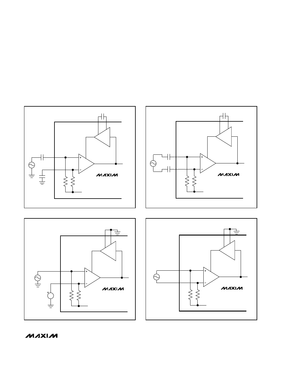
Figures 4 and 5 show single-ended and differential DC-
coupled input circuits for applications where a DC com-
ponent of the input signal is present. The amplifiers’
input common-mode voltage range extends from 1.75V
to 2.75V. To prevent attenuation of the input signal’s DC
component when operating in this mode, disable the off-
set-correction amplifier by grounding the _OCC+ and
_OCC- pins for the I and Q blocks (Figures 4 and 5).
ADCs
The I and Q ADC blocks receive the analog signals
from the respective I and Q input amplifiers. The ADCs
use flash conversion with 63 fully differential compara-
tors to digitize the analog input signal into a 6-bit output
in offset binary format.
MAX1002
Low-Power, 60Msps, Dual, 6-Bit ADC
_______________________________________________________________________________________
7
Figure 2. Single-Ended AC-Coupled Input
Figure 3. Differential AC-Coupled Input
Figure 4. Single-Ended DC-Coupled Input
Figure 5. Differential DC-Coupled Input
MAX1002
INPUT
AMP
20k
2.35V INTERNAL REFERENCE
20k
_IN+
_OCC+
_OCC-
_IN-
0.1
µ
F
0.22
µ
F
V
SOURCE
0.1
µ
F
OFFSET
CORREC-
TION
(ONE CHANNEL SHOWN)
MAX1002
INPUT
AMP
20k
2.35V INTERNAL REFERENCE
(ONE CHANNEL SHOWN)
20k
_IN+
_OCC+
_OCC-
_IN-
0.1
µ
F
0.1
µ
F
V
SOURCE
OFFSET
CORREC-
TION
0.22
µ
F
MAX1002
INPUT
AMP
20k
2.35V INTERNAL REFERENCE
20k
_IIN+
_IOCC+
_IOCC-
_IIN-
OFFSET-CORRECTION DISABLED
V
SOURCE
V
CM
1.75V TO 2.75V
(ONE CHANNEL SHOWN)
OFFSET
CORREC-
TION
MAX1002
INPUT
AMP
20k
2.35V INTERNAL REFERENCE
20k
_IIN+
_IOCC+
_IOCC-
_IIN-
OFFSET-CORRECTION DISABLED
V
SOURCE
DIFFERENTIAL SOURCE
WITH 1.75V TO 2.75V
COMMON-MODE
RANGE
(ONE CHANNEL SHOWN)
OFFSET
CORREC-
TION