Detailed description, Pin description, Table 1. input amplifier programming – Rainbow Electronics MAX1002 User Manual
Page 5
_______________Detailed Description
Converter Operation
The MAX1002 contains two 6-bit analog-to-digital con-
verters (ADCs), a buffered voltage reference, and oscil-
lator circuitry. The ADCs use a flash-conversion
technique to convert an analog input signal into a 6-bit
parallel digital output code. The MAX1002’s unique
design includes 63 fully differential comparators and a
proprietary encoding scheme that ensures no more
than 1LSB dynamic encoding error. The control logic
interfaces easily to most digital signal processors
(DSPs) and microprocessors (µPs) with +5V CMOS-
compatible logic interfaces. Figure 1 shows the
MAX1002 in a typical application.
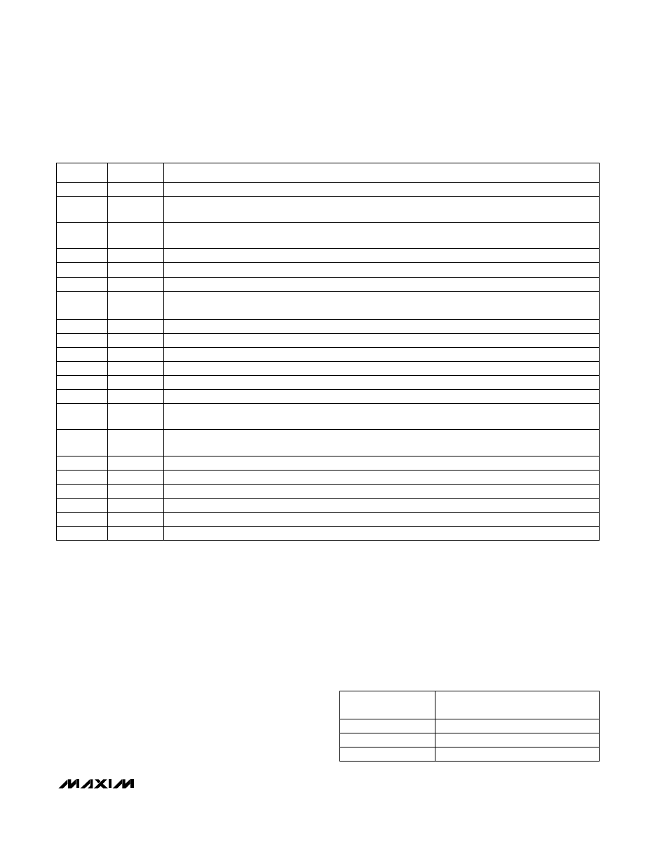
Programmable Input Amplifiers
The MAX1002 has in-phase (I) and quadrature (Q) pro-
grammable-gain input amplifiers with a 55MHz
-0.5dB bandwidth and true differential inputs. To maxi-
mize performance in high-speed systems, each amplifier
has less than 5pF of input capacitance. The input ampli-
fier gain is programmed via the GAIN pin to provide
three possible input full-scale ranges (FSR) (Table 1).
MAX1002
Low-Power, 60Msps, Dual, 6-Bit ADC
_______________________________________________________________________________________
5
______________________________________________________________Pin Description
PIN
Gain-Select Input. Sets input full-scale range: 125/250/500mVp-p (Table 1).
GAIN
1
FUNCTION
NAME
Positive I-Channel Offset-Correction Compensation. Connect 0.22µF capacitor
for AC-coupled inputs (Figures 2, 3). Ground for DC-coupled inputs (Figures 4, 5).
IOCC+
2
I-Channel Noninverting Analog Input
IIN+
4
Negative I-Channel Offset-Correction Compensation. Connect 0.22µF capacitor
for AC-coupled inputs (Figures 2, 3). Ground for DC-coupled inputs (Figures 4, 5).
IOCC-
3
+5V ±5% Supply. Bypass with 0.01µF capacitor to GND (Pin 7).
V
CC
6
+5V ±5% Supply. Bypass with 0.01µF capacitor to GND (Pin 11).
V
CC
8
Analog Ground
GND
7, 11, 12,
18, 19
I-Channel Inverting Analog Input
IIN-
5
Negative Oscillator/Clock Input
TNK-
10
Q-Channel Inverting Analog Input
QIN-
14
+5V ±5% Supply. Bypass with 0.01µF capacitor to GND (Pin 12).
V
CC
13
Negative Q-Channel Offset-Correction Compensation. Connect 0.22µF capacitor
for AC-coupled inputs (Figures 2, 3). Ground for DC-coupled inputs (Figures 4, 5).
QOCC-
16
Q-Channel Digital Outputs 0–5. DQ5 is the most significant bit (MSB).
DQ5–DQ0
20–25
Positive Q-Channel Offset-Correction Compensation. Connect 0.22µF capacitor
for AC-coupled inputs (Figures 2, 3). Ground for DC-coupled inputs (Figures 4, 5).
QOCC+
17
Q-Channel Noninverting Analog Input
QIN+
15
Positive Oscillator/Clock Input
TNK+
9
Digital Output Ground
OGND
27
I-Channel Digital Outputs 0–5. DI5 is the most significant bit (MSB).
DI0–DI5
30–35
Digital Clock Output. Frames the output data.
DCLK
29
+5V ±5% Digital Supply. Bypass each with 47pF to OGND (Pin 27).
V
CCO
26, 28
+5V ±5% Supply. Bypass with 0.01µF to GND (Pin 19).
V
CC
36
250
Open
125
V
CC
GAIN
500
GND
INPUT FULL-SCALE RANGE
(mVp-p)
Table 1. Input Amplifier Programming