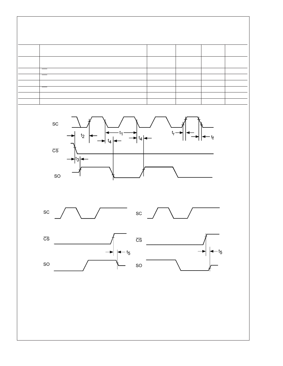
Figure 2. data output timing diagram, Figure 3. tri-state data output timing diagram, Logic electrical characteristics – Rainbow Electronics LM71 User Manual
Page 5: Lm71
Logic Electrical Characteristics
(Continued)
SERIAL BUS DIGITAL SWITCHING CHARACTERISTICS Unless otherwise noted, these specifications apply for V
+
= 2.65V
to 3.6V (Note 6); C
L
(load capacitance) on output lines = 100 pF unless otherwise specified. Boldface limits apply for T
A
= T
J
= T
MIN
to T
MAX
; all other limits T
A
= T
J
= +25˚C, unless otherwise noted.
Symbol
Parameter
Conditions
Typical
Limits
Units
(Limit)
t
1
SC (Clock) Period
0.16
DC
µs (min)
(max)
t
2
CS Low to SC (Clock) High Set-Up Time
100
ns (min)
t
3
CS Low to Data Out (SO) Delay
70
ns (max)
t
4
SC (Clock) Low to Data Out (SO) Delay
70
ns (max)
t
5
CS High to Data Out (SO) TRI-STATE
200
ns (max)
t
6
SC (Clock) High to Data In (SI) Hold Time
50
ns (min)
t
7
Data In (SI) Set-Up Time to SC (Clock) High
30
ns (min)
20031704
FIGURE 2. Data Output Timing Diagram
20031705
FIGURE 3. TRI-STATE Data Output Timing Diagram
LM71
www.national.com
5