Absolute maximum ratings, Operating ratings, Temperature-to-digital converter characteristics – Rainbow Electronics LM71 User Manual
Page 4: Logic electrical characteristics, Lm71
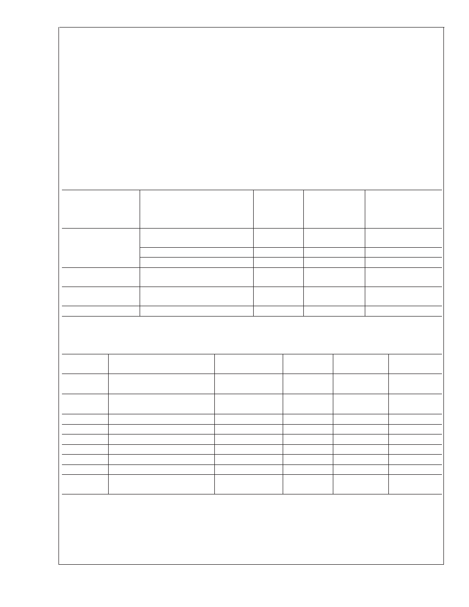
Absolute Maximum Ratings
Supply Voltage
−0.3V to 6.0V
Voltage at any Pin
−0.3V to V
+
+ 0.3V
Input Current at any Pin (Note 2)
5 mA
Storage Temperature
−65˚C to +150˚C
Soldering Information, Lead Temperature
SOT23-5 Package (Note 3)
Vapor Phase (60 seconds)
Infrared (15 seconds)
215˚C
220˚C
LLP-6 Package (Note 3)
Infrared (5 seconds)
215˚C
ESD Susceptibility (Note 4)
Human Body Model
Machine Model
2000V
200V
Operating Ratings
Specified Temperature Range
T
MIN
to T
MAX
LM71CIMF, LM71CISD
−40˚C to +150˚C
Supply Voltage Range (+V
S
)
LM71CIMF, LM71CISD
+2.65V to +5.5V
Temperature-to-Digital Converter Characteristics
Unless otherwise noted, these specifica-
tions apply for V
+
= 2.65V to 3.6V (Note 6). Boldface limits apply for T
A
= T
J
= T
MIN
to T
MAX
; all other limits T
A
= T
J
=
+25˚C, unless otherwise noted.
Parameter
Conditions
Typical
LM71CIMF
LM71CISD
Limits
Units
(Limit)
Temperature Error
T
A
= −10˚C to +65˚C
±
1.5
˚C (max)
T
A
= −40˚C to +85˚C
±
2.0
˚C (max)
T
A
= −40˚C to +150˚C
+3/−2
˚C (max)
Resolution
14
0.03125
Bits
˚C
Temperature
Conversion Time
200
270
ms (max)
Quiescent Current
Serial Bus Inactive
300
550
µA (max)
Logic Electrical Characteristics
DIGITAL DC CHARACTERISTICS Unless otherwise noted, these specifications apply for V
+
= 2.65V to 3.6V (Note 6). Bold-
face limits apply for T
A
= T
J
= T
MIN
to T
MAX
; all other limits T
A
= T
J
= +25˚C, unless otherwise noted.
Symbol
Parameter
Conditions
Typical
Limits
Units
(Limit)
V
IN(1)
Logical “1” Input Voltage
V
+
x 0.7
V (min)
V
+
+ 0.3
V (max)
V
IN(0)
Logical “0” Input Voltage
−0.3
V (min)
V
+
x 0.3
V (max)
Input Hysteresis Voltage
V
+
= 3.0V to 3.6V
0.4
0.33
V (min)
I
IN(1)
Logical “1” Input Current
V
IN
= V
+
0.005
3.0
µA (max)
I
IN(0)
Logical “0” Input Current
V
IN
= 0V
−0.005
−3.0
µA (min)
C
IN
All Digital Inputs
20
pF
V
OH
High Level Output Voltage
I
OH
= −400 µA
2.4
V (min)
V
OL
Low Level Output Voltage
I
OL
= +2 mA
0.4
V (max)
I
O_TRI-STATE
TRI-STATE
®
Output Leakage
Current
V
O
= GND
V
O
= V
+
−1
+1
µA (min)
µA (max)
LM71
www.national.com
4