Electrical characteristics (continued) – Rainbow Electronics MAX107 User Manual
Page 5
MAX107
Dual, 6-Bit, 400Msps ADC with On-Chip,
Wideband Input Amplifier
_______________________________________________________________________________________
5
Note 1:
INL and DNL is measured using a sine-histogram method.
Note 2:
Input offset is the voltage required to cause a transition between codes 0 and -1.
Note 3:
Numbers provided are for DC-coupled case. The user has the choice of AC-coupling, in which case, the DC input voltage
level does not matter.
Note 4:
The peak-to-peak input voltage required, causing a full-scale digitized output when using a trigonometric curve-fitting algo
rithm (e.g. FFT).
Note 5:
Guaranteed by design and characterization.
Note 6:
Common-mode rejection ratio is defined as the ratio of the change in the offset voltage to the change in the common-mode
voltage expressed in dB.
Note 7:
Measured with analog power supplies tied to the same potential.
Note 8:
Effective number of bits (ENOB) is computed from a curve-fit referenced to the theoretical full-scale range.
Note 9:
The clock and input frequencies are chosen so that there are 2041 cycles in an 8,192-long record.
Note 10: Signal-to-noise-ratio (SNR) is measured both with the other channel idling and converting an out-of-phase signal.
The worst case number is presented. Harmonic distortion components two through five are excluded from the noise.
Note 11: Harmonic distortion components two through five are included in the total harmonic distortion specification.
Note 12: Both I and Q inputs are effectively tied together (e.g. driven by power splitter). Signal amplitude is -0.5dB FS at an input
frequency of f
IN
= 124.999 MHz.
Note 13: Measured with a differential probe, 1pF capacitance.
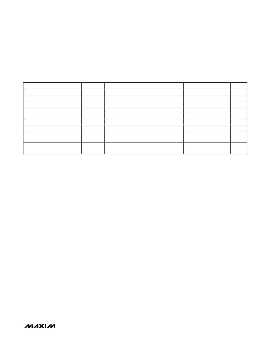
ELECTRICAL CHARACTERISTICS (continued)
(AV
CC
= AV
CC
I = AV
CC
Q = AV
CC
R = +5V, OV
CC
I = OV
CC
Q = +3.3V, AGND = AGNDI = AGNDQ = AGNDR = 0, OGNDI = OGNDQ
= 0, f
CLK
= 401.408MHz, C
L
= 1µF to AGND at REF, R
L
= 100
Ω ±1% applied to digital LVDS outputs, T
A
= T
MIN
to T
MAX
, unless
otherwise noted. Typical values are at T
A
= +25
°C)
PARAMETER
SYMBOL
CONDITIONS
MIN
TYP
MAX
UNITS
DREADY Duty Cycle
(Notes 5, 13)
47
53
%
LVDS Output Rise-Time
t
RDATA
20% to 80% (Notes 5, 13)
200
500
ps
LVDS Output Fall-Time
t
FDATA
20% to 80% (Notes 5, 13)
200
500
ps
Any differential pair
<65
LVDS Differential Skew
t
SKEW1
Any tw o LV D S outp ut si g nal s excep t D RE AD Y <100
ps
DREADY Rise-Time
t
RDREADY
20% to 80% (Notes 5, 13)
200
500
ps
DREADY Fall-Time
t
FDREADY
20% to 80% (Notes 5, 13)
200
500
ps
Primary Port Pipeline Delay
t
PDP
5
Clock
Cycles
Auxiliary Port Pipeline Delay
t
PDA
6
Clock
Cycles